Structure and method for a triple-gate transistor with reverse sti

a technology of reverse sti and transistor, applied in the direction of semiconductor devices, basic electric elements, electrical equipment, etc., can solve the problems of reducing the degree to which transistor dimensions can be reliably scaled, reducing the drain induced barrier (dibl), and/or increasing the off-state current du

Active Publication Date: 2008-10-30
TEXAS INSTR INC
View PDF34 Cites 5 Cited by
  • Summary
  • Abstract
  • Description
  • Claims
  • Application Information

AI Technical Summary

Problems solved by technology

These devices overcome performance and process limitations of conventional planar transistor devices due to a reduction in gate length accompanied with scale down.
However, current photolithographic and etching techniques generally limit the extent to which transistor dimensions can be reliably scaled.
In addition, as the gate length is reduced, the transistor performance can be inhibited by short channel effects, which can lead to an increased drain induced barrier lowering (DIBL), and / or an increased off-state current due to the threshold voltage (Vt) roll off.
In practice, however, the conventional multi-gate approaches have suffered from cost and performance shortcomings, because SOI wafers are more expensive than ordinary silicon substrates and because the channel surface has been etched while carving the upper SOI silicon layer into islands or blocks.
This reduces the carrier mobility and degrades the device performance.
Problems arise, however, since recessing the STI exposes the silicon substrate at the sidewall of the substrate.
As a result of the insufficient gate wrap, device performance degrades, especially as the devices are scaled down.

Method used


Image

  • Structure and method for a triple-gate transistor with reverse sti
  • Structure and method for a triple-gate transistor with reverse sti
  • Structure and method for a triple-gate transistor with reverse sti

Examples


Embodiment Construction

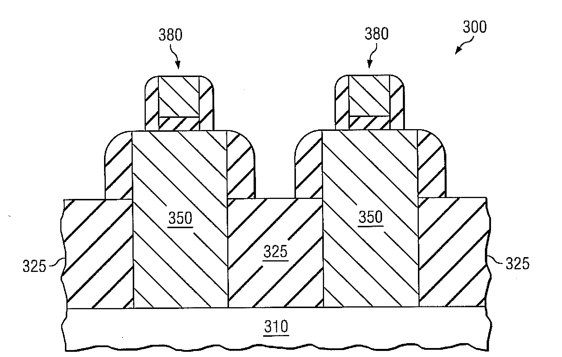
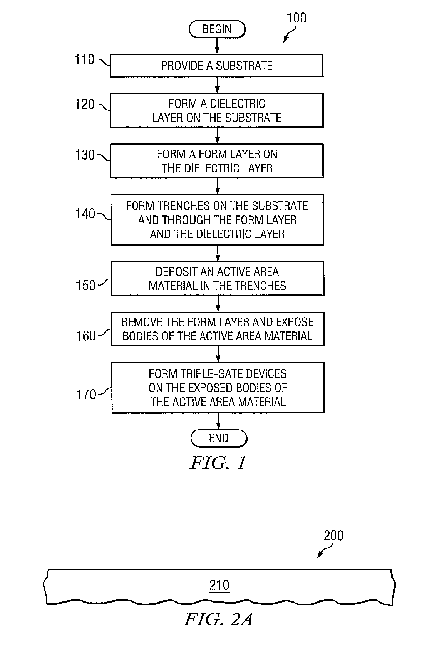
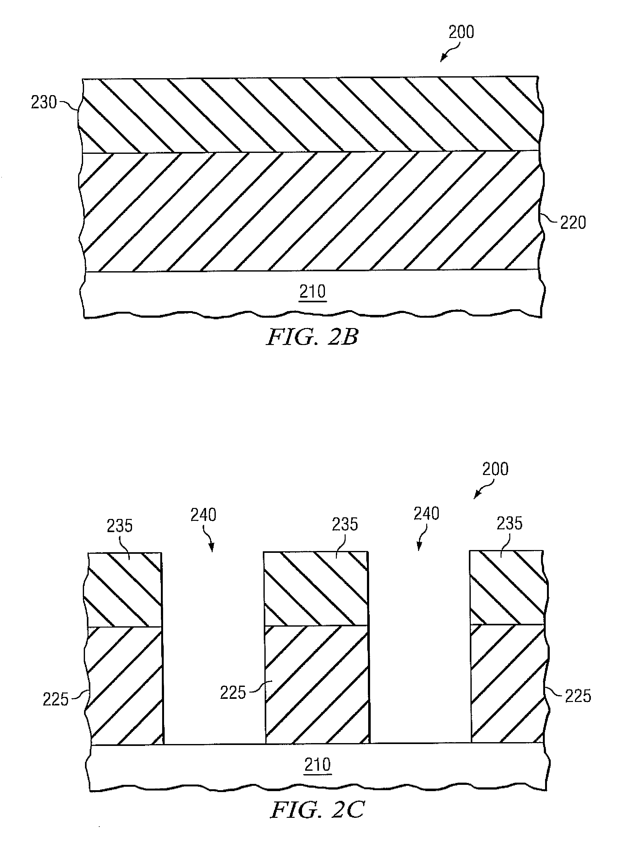
[0017]Reference will now be made in detail to exemplary embodiments of the invention, an example of which is illustrated in the accompanying drawings. Wherever possible, the same reference numbers will be used throughout the drawings to refer to the same or like parts. In the following description, reference is made to the accompanying drawings that form a part thereof, and in which is shown by way of illustration specific exemplary embodiments in which the invention may be practiced. These embodiments are described in sufficient detail to enable those skilled in the art to practice the invention and it is to be understood that other embodiments may be utilized and that changes may be made without departing from the scope of the invention. The following description is, therefore, merely exemplary.

[0018]While the invention has been illustrated with respect to one or more implementations, alterations and / or modifications can be made to the illustrated examples without departing from t...


PUM


Abstract

Exemplary embodiments provide triple-gate semiconductor devices isolated by reverse STI structures and methodologies for their manufacture. In an exemplary process, stacked layers including a form layer over a dielectric layer can be formed over a semiconductor substrate. One or more trenches can be formed by etching through the stacked layers. The one or more trenches can be filled by an active area material to form one or more active areas, which can be isolated by remaining portions of the dielectric layer. Bodies of the active area material can be exposed by removing the form layer. One or more triple-gate devices can then be formed on the exposed active area material. The exemplary triple-gate semiconductor devices can control the dimensions for the active areas and provide less isolation spacing between the active areas, which optimizes manufacturing efficiency and device integration quality.

Description

FIELD OF THE INVENTION[0001]This invention relates generally to semiconductor devices, and, more particularly, to triple-gate transistors and methods for their manufacture.BACKGROUND OF THE INVENTION[0002]Multi-gate transistors have been developed for next-generation devices. Exemplary multi-gate transistor designs include dual-gate and triple-gate transistors as well as quad-gate transistors and “PI”-gate transistors. These devices overcome performance and process limitations of conventional planar transistor devices due to a reduction in gate length accompanied with scale down.[0003]For example, the length of the gate structure is typically the smallest dimension of conventional planar MOS transistors in order to increase device density, improve performance (e.g., increase switching speed), and to reduce power consumption. However, current photolithographic and etching techniques generally limit the extent to which transistor dimensions can be reliably scaled. In addition, as the ...

Claims


Application Information

Patent Timeline
Patent Type & Authority Applications(United States)
IPC IPC(8): H01L21/336
CPCH01L29/66795H01L29/7851
Inventor CHAMBERS, JAMES JOSEPHVISOKAY, MARK ROBERT
Owner TEXAS INSTR INC
Why Eureka
Try Eureka