Multi-bit programming device and method of multi-bit programming

Active Publication Date: 2008-11-06
SAMSUNG ELECTRONICS CO LTD
View PDF9 Cites 17 Cited by
  • Summary
  • Abstract
  • Description
  • Claims
  • Application Information

AI Technical Summary

Benefits of technology

[0011]Example embodiments of present invention may provide a multi-bit programming device and method which may reduce an error generated while. T

Problems solved by technology

Accordingly, controlling a gradation of a th

Method used


Image

  • Multi-bit programming device and method of multi-bit programming
  • Multi-bit programming device and method of multi-bit programming
  • Multi-bit programming device and method of multi-bit programming

Examples


Example

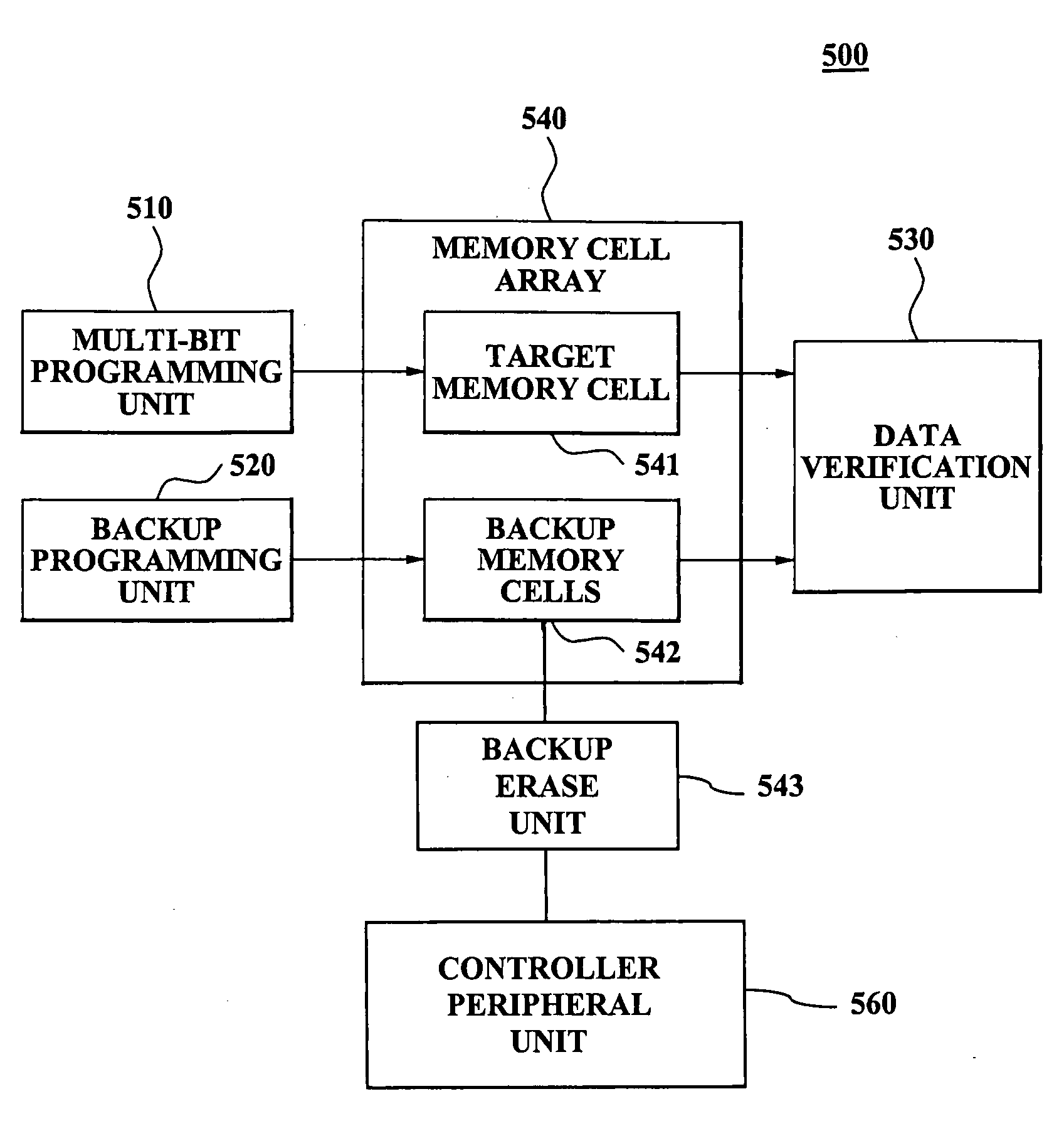
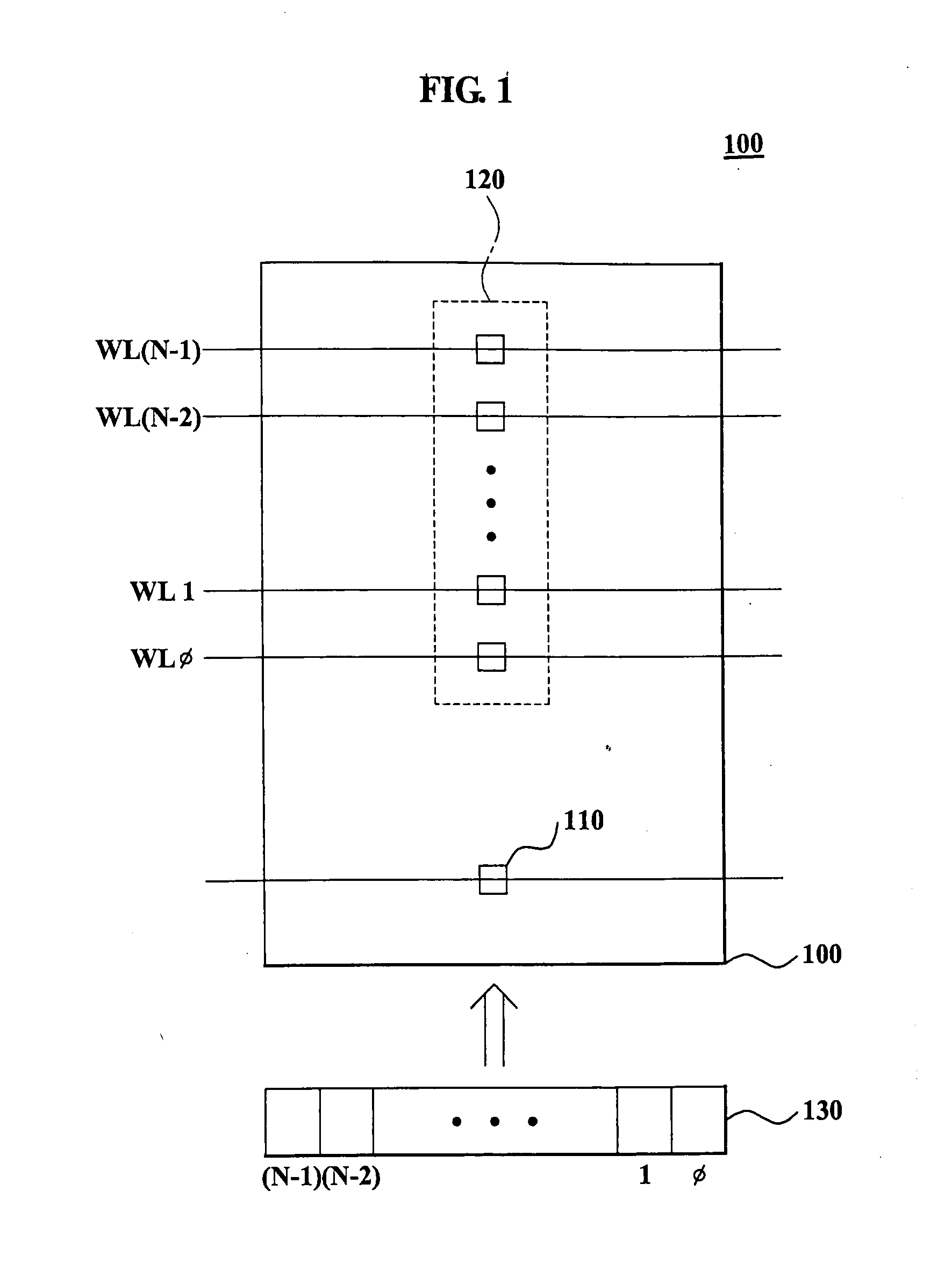
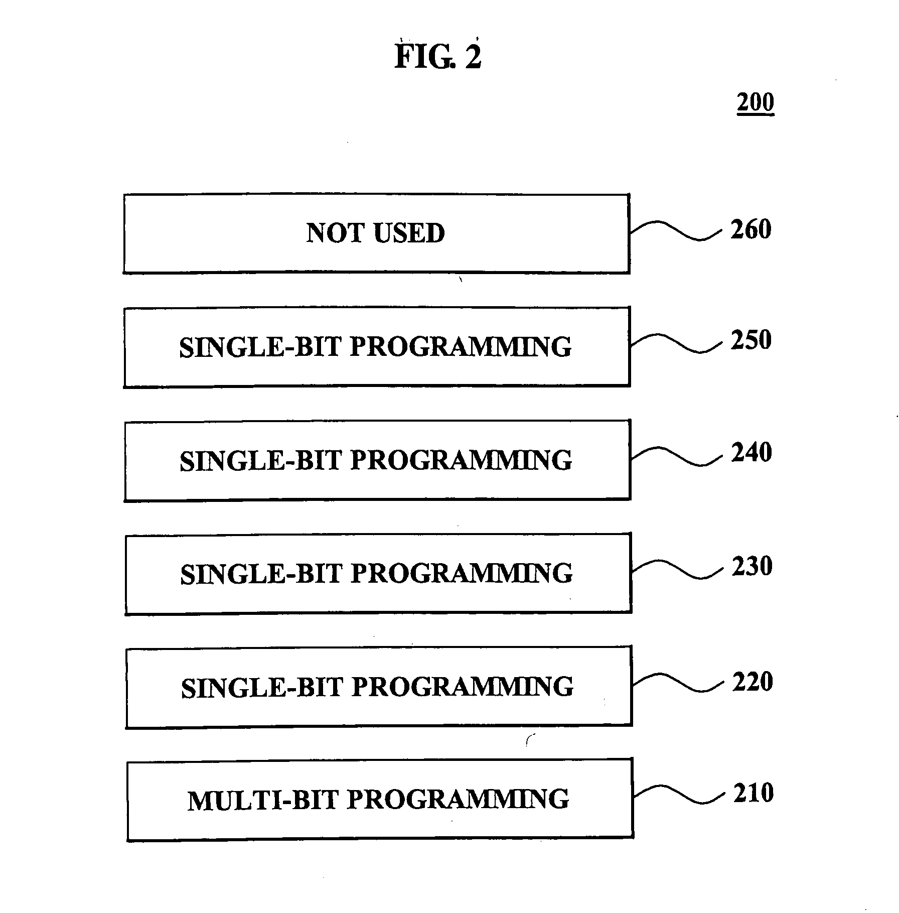
[0021]Reference will now be made in detail to example embodiments of the present invention, examples of which are illustrated in the accompanying drawings, wherein like reference numerals refer to the like elements throughout.

[0022]It will be understood that when an element or layer is referred to as being “on”, “connected to” or “coupled to” another element or layer, it may be directly on, connected or coupled to the other element or layer or intervening elements or layers may be present. In contrast, when an element is referred to as being “directly on,”“directly connected to” or “directly coupled to” another element or layer, there may be no intervening elements or layers present. As used herein, the term “and / or” includes any and all combinations of one or more of the associated listed items.

[0023]It will be understood that, although the terms first, second, third etc. may be used herein to describe various elements, components, regions, layers and / or sections, these elements, c...


PUM


Abstract

A multi-bit programming device and method for a non-volatile memory are provided. In one example embodiment, a multi-bit programming device may include a multi-bit programming unit configured to multi-bit program original multi-bit data to a target memory cell in a memory cell array, and a backup programming unit configured to select backup memory cells in the memory cell array with respect to each bit of the original multi-bit data, and program each bit of the original multi-bit data to a respective one of the selected backup memory cells.

Description

PRIORITY CLAIM[0001]A claim of priority is made to Korean Patent Application No. 10-2007-0042764, filed on May 2, 2007, in the Korean Intellectual Property Office, the disclosure of which is incorporated herein by reference.BACKGROUND[0002]1. Field[0003]Example embodiments of the present invention may relate to a semiconductor memory device, and more particularly, to a multi-bit programming device and a method of multi-bit programming.[0004]2. Description of Related Art[0005]A non-volatile memory (NVM) device is a type of memory, which can electrically program and erase, and maintain programmed data even when power is not supplied thereto.[0006]NVM devices are widely used for digital cameras, cellular phones, personal data assistants (PDAs), laptop computers, and the like. Also, an NVM device is capable of storing a large amount of data in a relatively small package.[0007]In general, an NVM device programs and erases data by changing a threshold voltage of a transistor in a memory c...

Claims


Application Information

Patent Timeline
IPC IPC(8): G11C7/00
CPCG11C11/5628G11C2211/5621G11C2211/5641G11C16/10G11C16/04
Inventor BYUN, SUNG-JAECHAE, DONG HYUKCHO, KYOUNG LAEKONG, JUN JINLEE, YOUNG HWANLEE, SEUNG JAEJO, NAM PHILKANG, DONG KU
Owner SAMSUNG ELECTRONICS CO LTD
Why Eureka
Try Eureka