Non-volatile semiconductor memory device and method of manufacturing the same

Inactive Publication Date: 2008-11-20
KK TOSHIBA
View PDF4 Cites 75 Cited by
  • Summary
  • Abstract
  • Description
  • Claims
  • Application Information

AI Technical Summary

Benefits of technology

[0009]An aspect of the present invention provides a non-volatile semiconductor memory device, comprising: a plurality of memory cells, each including a semiconductor substrate, a first insulating film formed on the semiconductor substrate, a floating gate formed on the semiconductor substrate with the inclusion of the first insulating film, a second insulating film formed on the floating gate, and a control gate formed on the floating gate with the inclusion of the second insulating film; an element isolation insulating film formed in the semiconductor substrate and extending in a gate-length direction to isolate between memory cells adjoining in a gate-width direction; and an air gap formed on the element isolation insulating film and between floating gates adjoining in the gate-width direction.
[0010]Another aspect of the present invention provides a non-volatile semiconductor memory device, comprising: a memory cell array having a plurality of memory cell columns, which are arranged into a matrix on a semiconductor substrate, each having a plurality of memory cells, which are arranged in a first direction, each having a stacked-gate structure of a floating gate and a control gate stacked with a insulating layer disposed therebetween, the control gate extending in a second direction orthogonal to the first direction to form a word line which is commonly used by a plurality of memory cells adjoining in the second direction; and a shallow trench isolation formed in the semiconductor subs

Problems solved by technology

Such the EEPROM causes a problem associated with interference between floating gates due

Method used


Image

  • Non-volatile semiconductor memory device and method of manufacturing the same
  • Non-volatile semiconductor memory device and method of manufacturing the same
  • Non-volatile semiconductor memory device and method of manufacturing the same

Examples


first embodiment

Method of Manufacturing

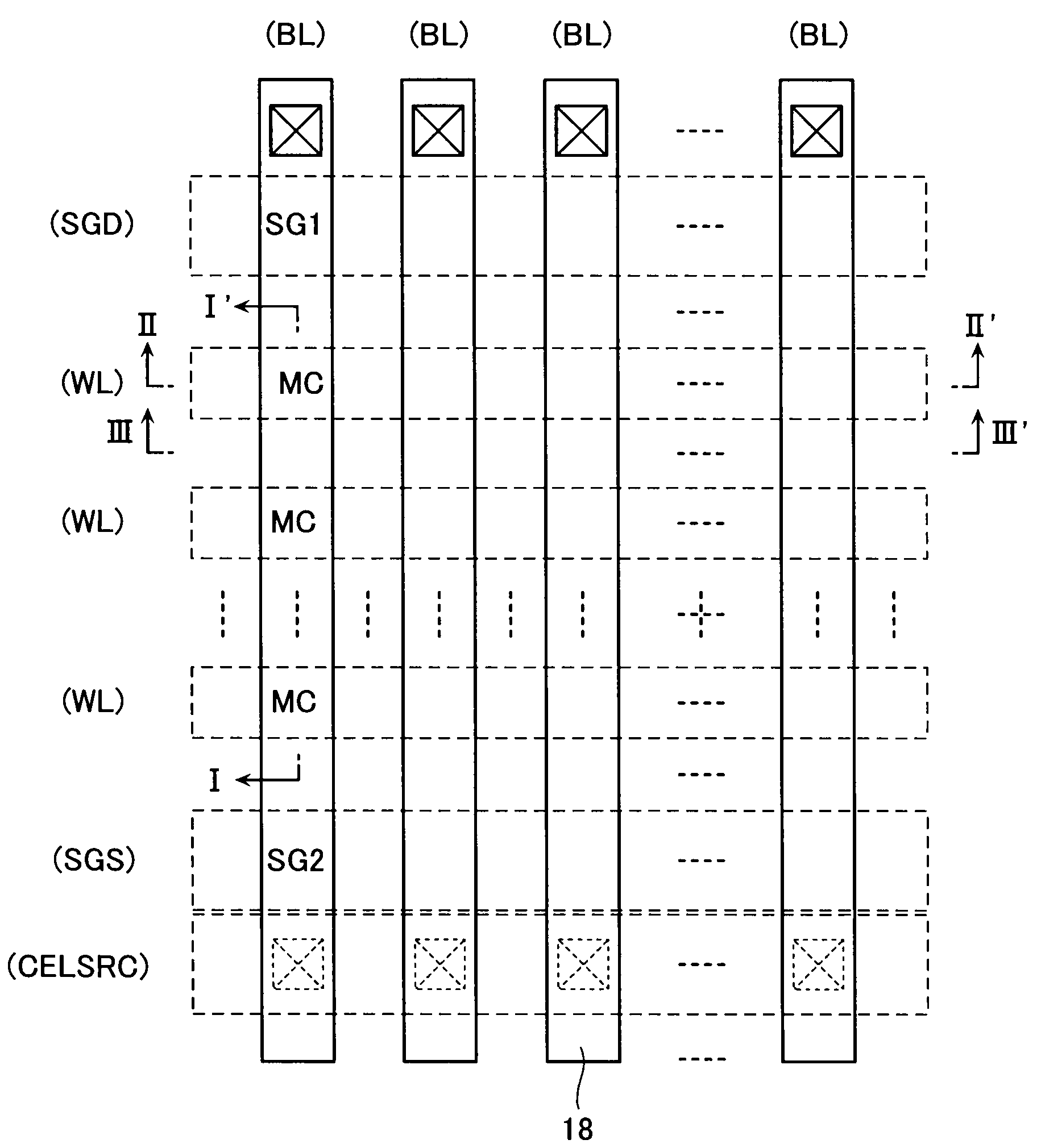
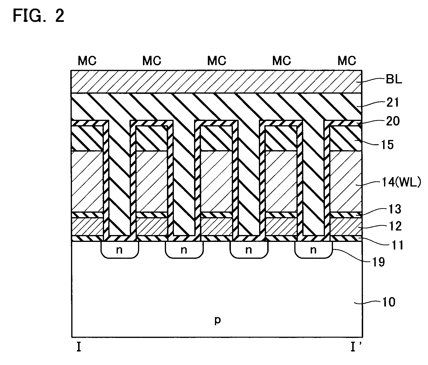
[0053]With reference to FIGS. 5-24, a method of manufacturing the NAND-type EEPROM according to the above first embodiment is described next.

[0054]First, as shown in FIG. 5, the gate oxide 11 is formed with a thickness of, for example, 10 nm on a memory cell region of the silicon substrate 10. A first polysilicon film 12A to be turned into the floating gate 12 is formed with a thickness of, for example, 100 nm on the gate oxide film 11. Further, a silicon nitride 30 is formed with a thickness of, for example, 50 nm on the first polysilicon film 12A. Then, a resist film 31 is formed on the silicon nitride 30. The resist film 31 is patterned as shown in FIG. 6 to selectively remove the silicon nitride 30, the first polysilicon film 12A, the gate oxide film 11 and an upper layer of the silicon substrate 10 by anisotropic etching to form the element isolation trenches 16.

[0055]Subsequently, as shown in FIG. 7, after removal of the resist film 31, a first buried fi...

second embodiment

Method of Manufacturing

[0073]FIG. 28 is a cross-sectional view of an NAND-type EEPROM according to another embodiment of the present invention taken along the word line WL in a process step.

[0074]In this embodiment, a process of CVD, for example, is applied to form an air-gap creation film 35 composed of a carbon-based material on the element isolation insulating film 17 in place of the air-gap creation film 32 of the polysilazan oxide or the like as shown in FIG. 9. Also in this case, the air-gap creation film 35 is formed over the entire surface. Then, it is polished by CMP with a stopper of the silicon nitride film 30, followed by a process of wet etching or RIE using DHF or the like to recess the air-gap creation film 35 back to a certain thickness.

[0075]The carbon-based air-gap creation film 35 can be removed by O2 ashing. Thus, the air-gap 22 can be formed in the portion where the carbon-based air-gap creation film 35 once existed.


PUM


Abstract

A non-volatile semiconductor memory device comprises a plurality of memory cells, each including a semiconductor substrate, a first insulating film formed on the semiconductor substrate, a floating gate formed on the semiconductor substrate with the inclusion of the first insulating film, a second insulating film formed on the floating gate, and a control gate formed on the floating gate with the inclusion of the second insulating film; an element isolation insulating film formed in the semiconductor substrate and extending in a gate-length direction to isolate between memory cells adjoining in a gate-width direction; and an air gap formed on the element isolation insulating film and between floating gates adjoining in the gate-width direction.

Description

CROSS-REFERENCE TO RELATED APPLICATION[0001]This application is based upon and claims the benefit of prior Japanese Patent Application No. 2007-127615, filed on May 14, 2007, the entire contents of which are incorporated herein by reference.BACKGROUND OF THE INVENTION[0002]1. Field of the Invention[0003]The present invention relates to a non-volatile semiconductor memory device with element isolation trenches formed to provide isolation between elements and method of manufacturing the same.[0004]2. Description of the Related Art[0005]Non-volatile semiconductor memory devices include electrically erasable programmable EEPROMs as known. In general, an EEPROM comprises memory cells each including a MOS transistor with a stacked-gate structure of a floating gate serving as a charge accumulation layer and a control gate stacked.[0006]Most suitable one for achieving large capacity among the EEPROMs is an NAND-type EEPROM. The NAND-type EEPROM comprises plural memory cells serially connect...

Claims


Application Information

Patent Timeline
IPC IPC(8): H01L29/788H01L21/336
CPCH01L21/7682H01L27/115H01L27/11521H01L29/4991H01L29/66825H01L21/28273H10B69/00H10B41/30H01L29/40114
Inventor KUNIYA, TAKUJI
Owner KK TOSHIBA
Why Eureka
Try Eureka