Display Apparatus
a technology of display apparatus and contact surface, which is applied in the field of display apparatus, can solve the problems of large distance between the display surface and the contact surface of the pen, attenuation of the electromagnetic field, and worsening the sensitivity of position detection, so as to achieve the effect of not easily broken and impairing the luminan
- Summary
- Abstract
- Description
- Claims
- Application Information
AI Technical Summary
Benefits of technology
Problems solved by technology
Method used
Image
Examples
example 1
[0103]In this example, the display apparatus according to First Embodiment of the present invention is prepared in the following manner.
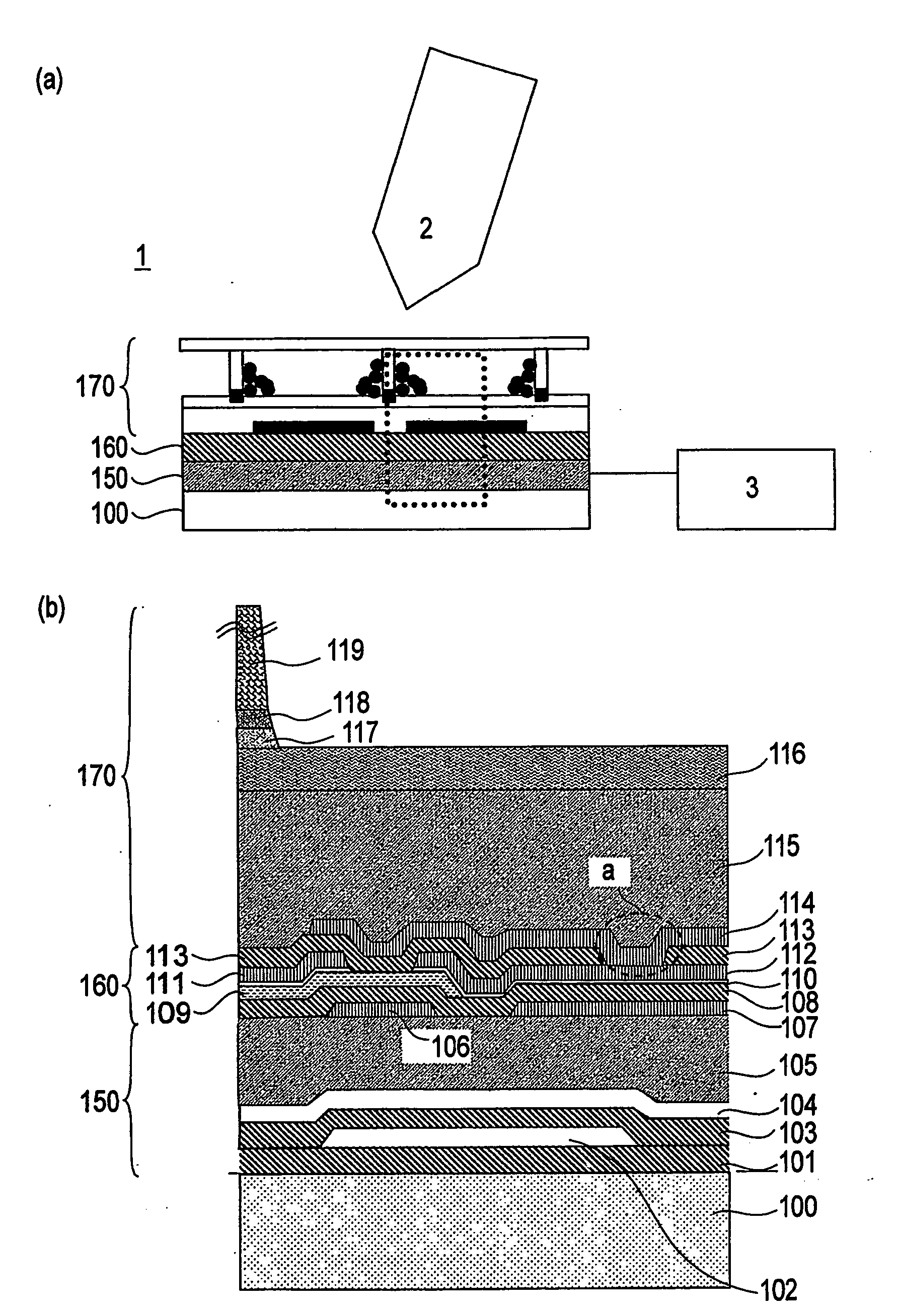
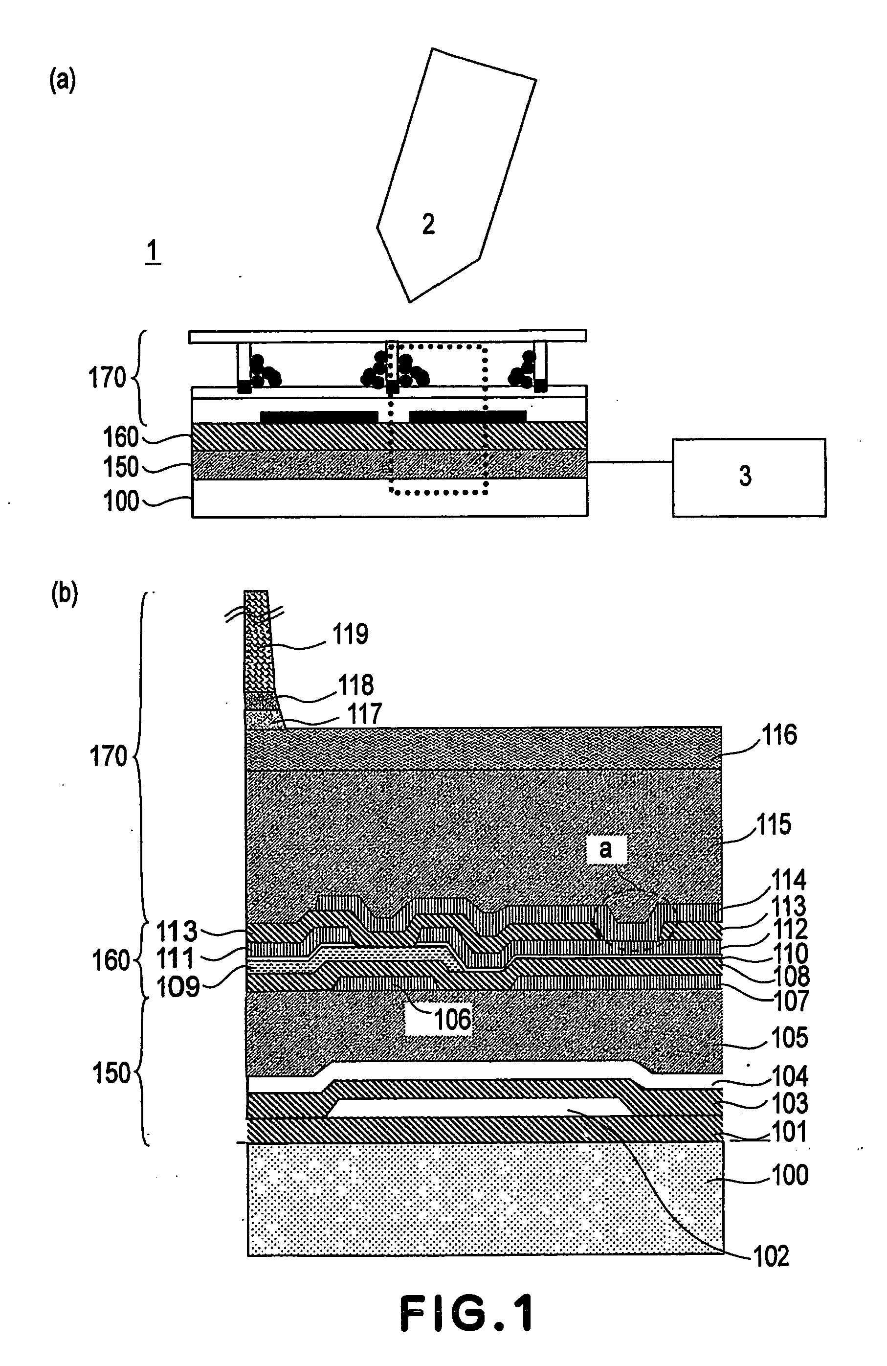
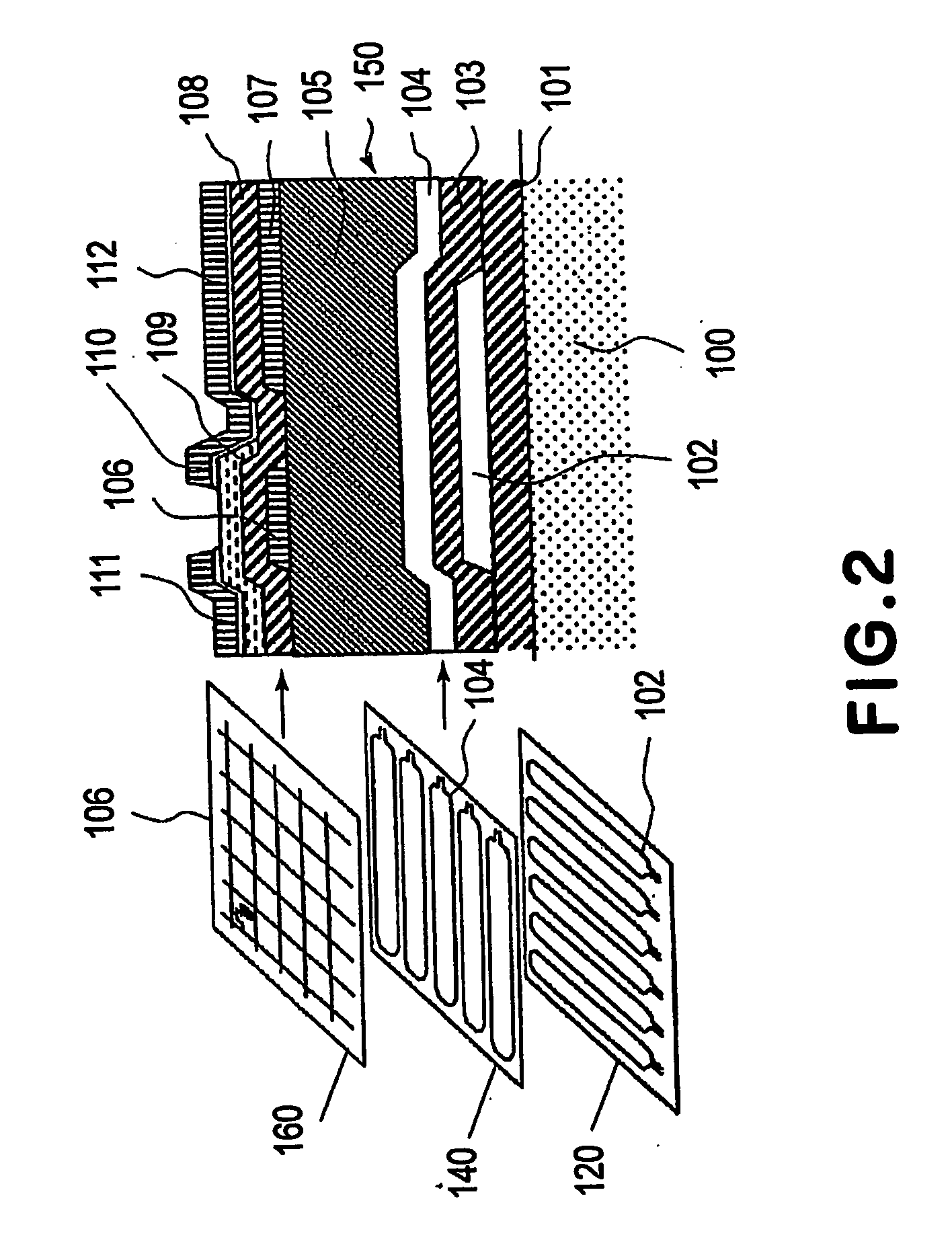
[0104]A substrate 100 is a thin electroconductive SUS foil or plate. An insulating film 101 disposed on the substrate 100 is formed of an insulating material such as SiN or a resin material. As wiring (metal coils) 102 and 104, a wiring material of Al which exhibits a low electric resistivity is used but in the case where there is a subsequent step includes a production process performed at a temperature exceeds a melting temperature of Al, a metal material such as Cr, Ta or Al—Nd is used instead of Al. Such a metal material is vapor-deposited on the insulating film by sputtering and thereon, a photoresist is applied and subjected to selective exposure and development, followed by etching of the metal film to form a loop-like wiring portion. As a TFT 109, a thin film of an amorphous semiconductor is used.
[0105]More specifically, the display apparatu...
example 2
[0127]In this example, the display apparatus of Second Embodiment of the present invention is prepared in the following manner.
[0128]First, the structure of display apparatus will be described with reference to FIG. 6.
[0129]In this example, a 100 μm-thick SUS sheet Al in which a multiplicity of through holes 4 are formed with an opening width of 20 μm, is used. Further, as an insulating liquid 15, it is possible to use a liquid principally comprising a paraffin-based hydrocarbon solvent. As charged electrophoretic particles 16, it is possible to use black particles of carbon black-containing polystyrene resin.
[0130]The SUS substrate A1 and the through holes 4 are coated and filled with an acrylic resin layer (thickness: 2 μm) for electrical insulation and smoothness. Further, it is also possible to use an SiN epoxy-based resin film instead of the acrylic resin. In the latter case, however, it is difficult to realize a film thickness of not less than 1 μm in CVD used when the SiN fil...
PUM
 Abstract
Description
Claims
Application Information


