

Bandgap circuit
- Summary
- Abstract
- Description
- Claims
- Application Information
AI Technical Summary
Benefits of technology
Problems solved by technology
Method used
Image

Examples
first embodiment
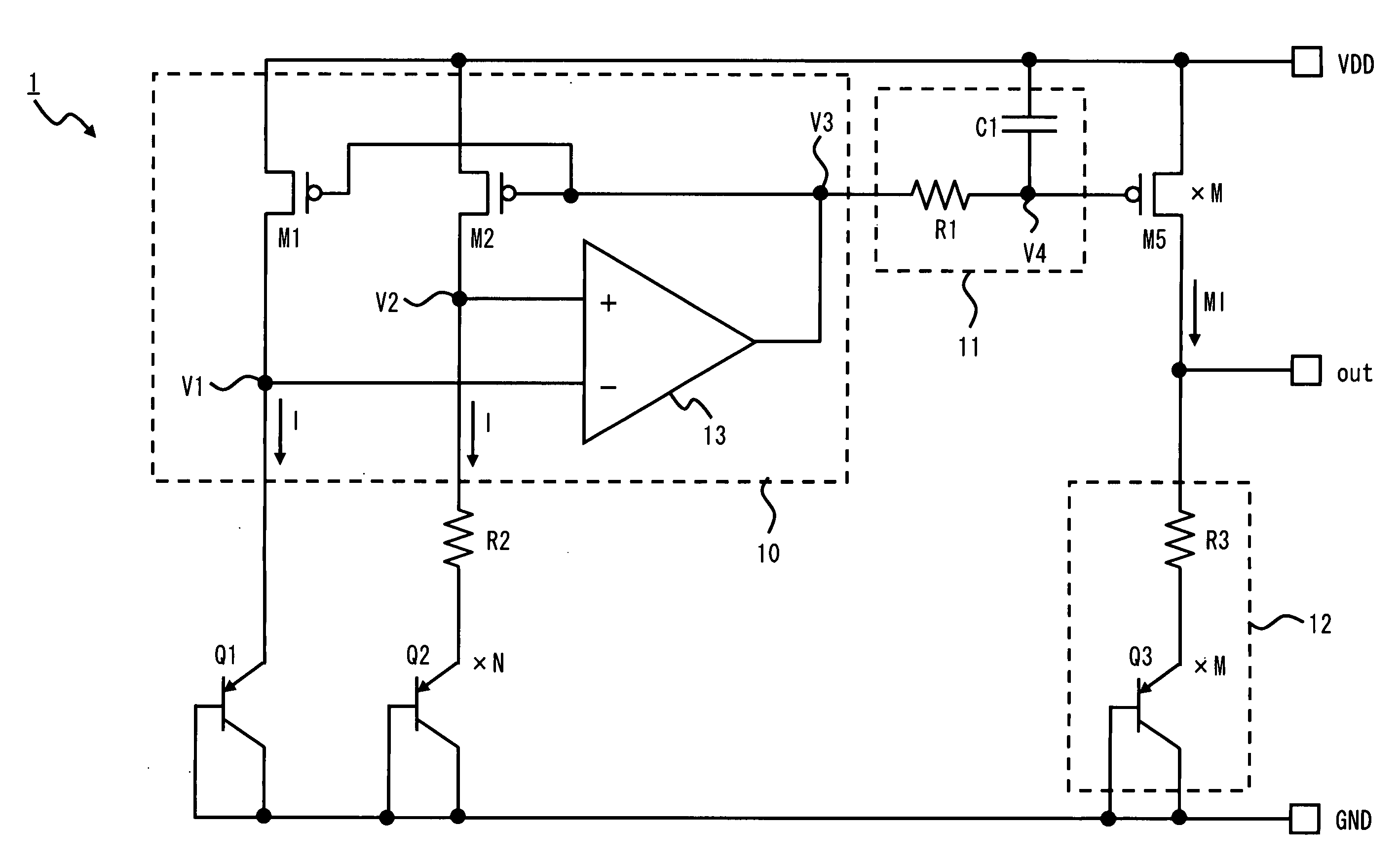
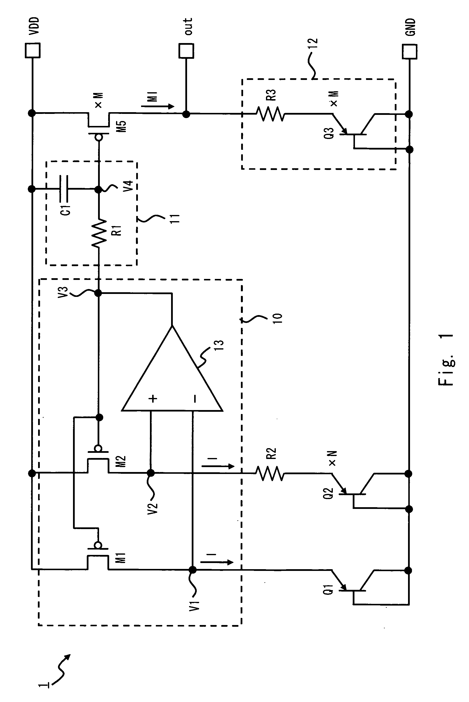
[0018]The embodiments of the present invention will be described hereinafter in detail with reference to the drawings. FIG. 1 shows a circuit diagram of a bandgap circuit 1 according to the first embodiment. As shown in FIG. 1, the bandgap circuit 1 includes a first diode element (PNP transistor Q2, for example), a second diode element (PNP transistor Q1, for example), a first resistor (resistor R2, for example), a control voltage generating part 10, a filter 11, an output transistor M5, and a load circuit 12. Note that the bandgap circuit 1 forms a control voltage generating circuit by the PNP transistors Q1 and Q2, the resistor R2, and the control voltage generating part 10.
[0019]The PNP transistor Q2 has a diode connection where a base and a collector are connected together. The PNP transistor Q2 includes an emitter (one end) formed by a P-type semiconductor region, a base formed by an N-type semiconductor region, and a collector (the other end) formed by a P-type semiconductor r...
second embodiment
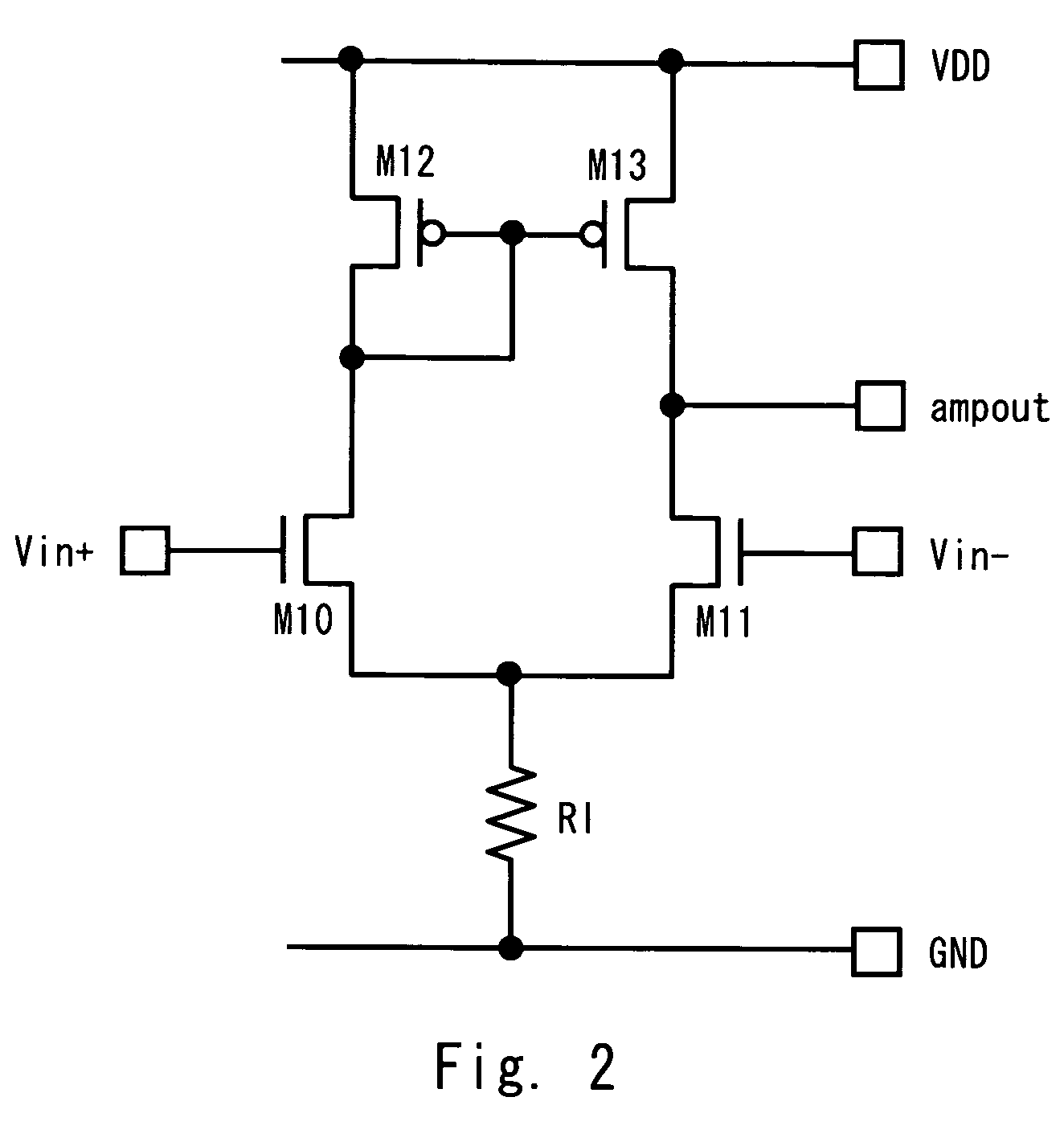
[0042]FIG. 4 shows a circuit diagram of the bandgap circuit 2 according to the second embodiment. The bandgap circuit 2 includes a control voltage generating part 20 in place of the control voltage generating part 10. The control voltage generating part 20 sets current flowing in the PMOS transistors M1 and M2 by two transistors without employing the amplifier 13. The control voltage generating part 20 includes a third transistor (NMOS transistor M4, for example) and a fourth transistor (NMOS transistor M3, for example) in place of the amplifier 13. The bandgap circuit 2 includes an activation circuit 21.
[0043]The NMOS transistor M3 has a source connected to the resistor R1, a drain connected to the PMOS transistor M2, and a gate connected to the NMOS transistor M4. The NMOS transistor M4 has a source connected to an emitter of the PNP transistor Q1, and a gate and a drain connected in common. In summary, the NMOS transistors M3 and M4 form a current mirror.
[0044]In the bandgap circ...
PUM
 Abstract
Description
Claims
Application Information