Organic light emitting display device and manufacturing method of the same

a technology of light-emitting display device and organic light-emitting diodes, which is applied in the direction of discharge tube luminescnet screen, paper/cardboard containers, containers, etc., can solve the problems of encapsulation substrate being in contact with organic light-emitting diodes and encapsulation substrate being damaged

Inactive Publication Date: 2009-01-08
SAMSUNG DISPLAY CO LTD
View PDF6 Cites 15 Cited by
  • Summary
  • Abstract
  • Description
  • Claims
  • Application Information

AI Technical Summary

Benefits of technology

[0010]It is another object of the present invention is to provide an organic light emitting display protecting organic light emitting diodes from external impacts, and a manufacturing method of the same.

Problems solved by technology

The organic light emitting display device, however, has problems that the encapsulation substrate may be in contact with organic light emitting diodes, or the encapsulation substrate be damaged by the external impacts because the distance between the deposition substrate and the encapsulation substrate is usually very small at a distance of 10 μm to 20 μm if the encapsulation substrate is provided in a substrate form as described above.

Method used


Image

  • Organic light emitting display device and manufacturing method of the same
  • Organic light emitting display device and manufacturing method of the same
  • Organic light emitting display device and manufacturing method of the same

Examples


first embodiment

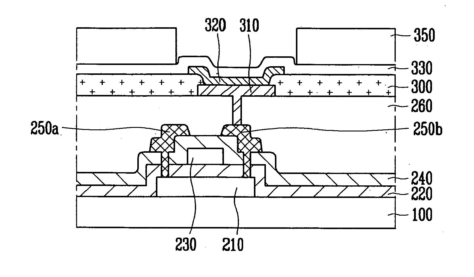
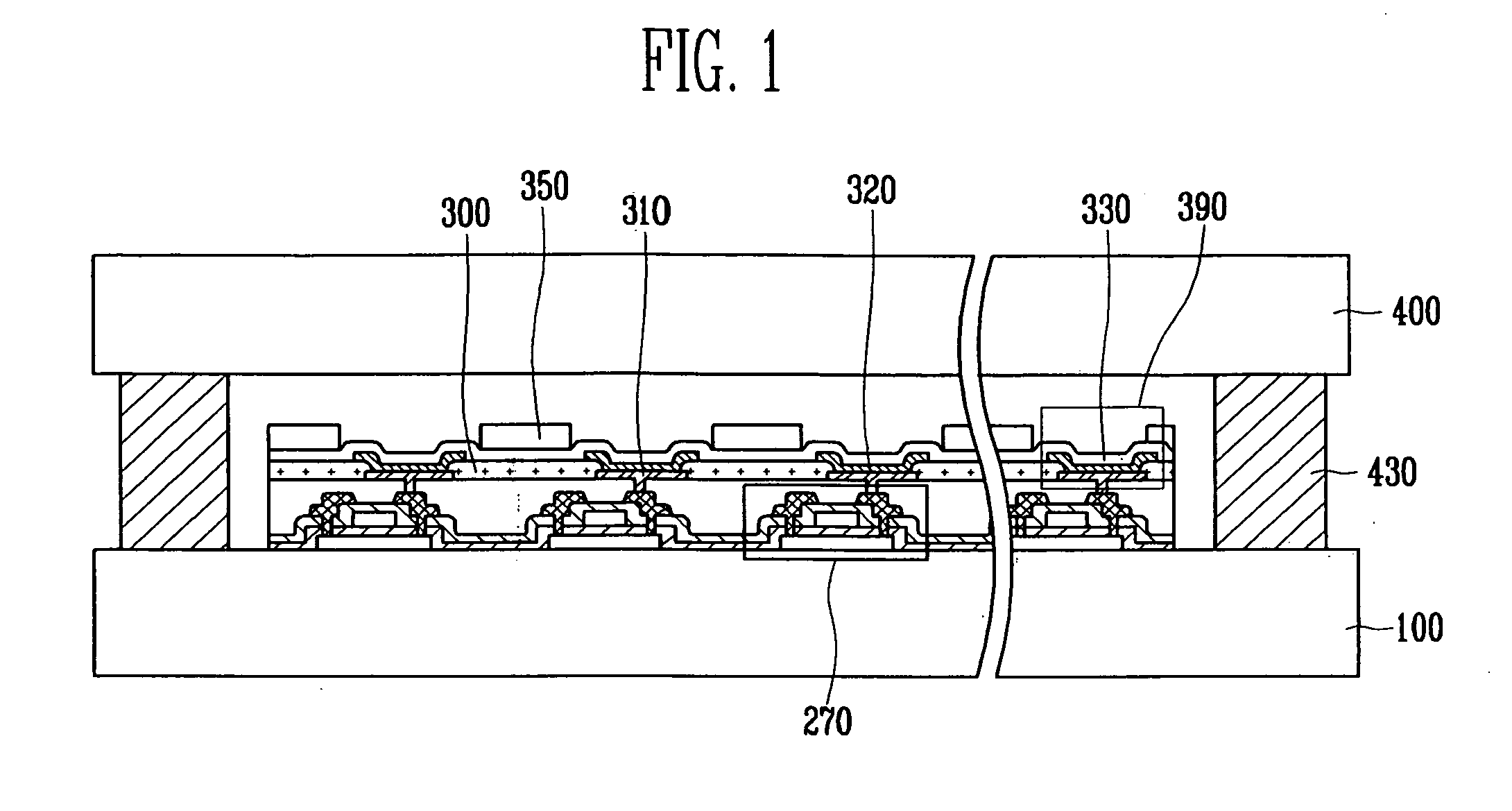
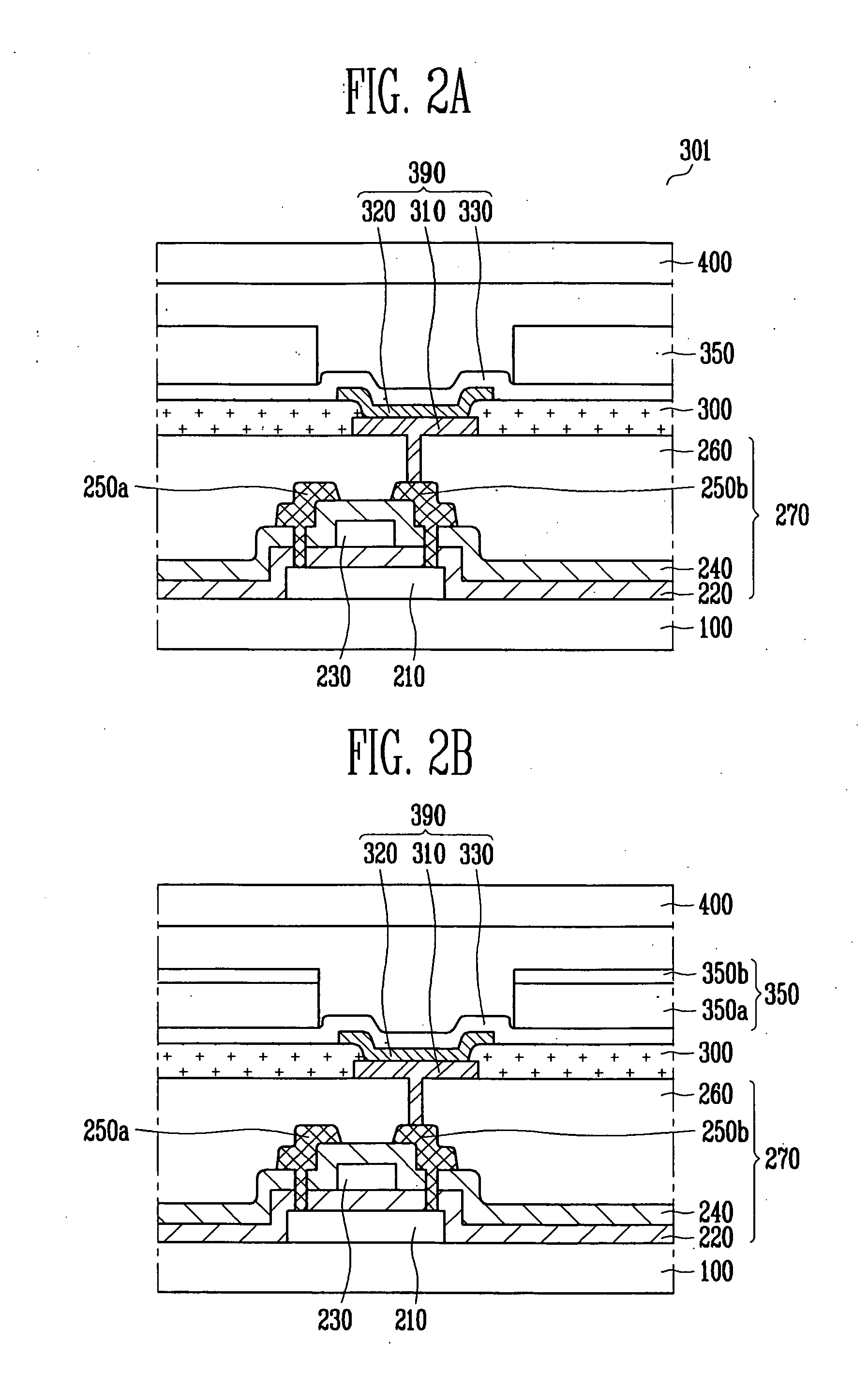
[0032]Therefore, if such an etching glass is used as the encapsulation substrate, a problem that first substrate 100 and second substrate 410 are in contact with each other when external impacts is applied to the spacer may be rather relieved, compared to the In this case, spacer 350 maybe provided between first substrate 100 and second substrate 410 to prevent the contact of second substrate 410 with the organic light emitting diode. In this case, spacer 350 containing a desiccant has functions to absorb internally penetrated moisture, and spacer 350 serves to easily manufacture an organic light emitting display device without attaching an extra desiccant. Spacer 350 may also have a configuration that a separate desiccant layer is formed on a base, or main material layer composed of acryl or polyimide.

[0033]In this case, the employed desiccant maybe one selected from the group consisting of CaO, MgO and BaO. Here, spacer 350 may be formed at a height of 3 μm to 5 μm, and spacer 35...

second embodiment

[0034]In the case of the second embodiment, a sealing member 440 is applied onto a region where second substrate 410 is in contact with first substrate 100, and then cured.

third embodiment

[0035]FIG. 4 is a cross-sectional view showing an organic light emitting display device according to the present invention.

[0036]The third embodiment that is distinct from the first embodiment is characterized in that the organic light emitting display device includes a spacer 360 containing a desiccant, wherein spacer 360 is not formed on first substrate 100, but provided in second substrate 400. Spacer 360 may also have a configuration that a separate desiccant layer is formed on a base, or main material layer composed of acryl or polyimide.

[0037]That is, spacer 360 is provided in second substrate 400 which is an encapsulation substrate 400, wherein spacer 360 is disposed in a position in which a path of the light emitted from the organic light emitting diodes is not hindered. For example, spacer 360 may be disposed between organic thin film layers 320 formed on first substrate 100.

[0038]FIG. 5 to FIG. 8 are cross-sectional views illustrating a method of manufacturing an organic l...


PUM

PropertyMeasurementUnit
distanceaaaaaaaaaa
heightaaaaaaaaaa
fluorescentaaaaaaaaaa

Abstract

An organic light emitting display device having spacers and a manufacturing method thereof. The organic light emitting display device according to the present invention includes a first substrate divided into a pixel region and a non-pixel region surrounding the pixel region; a plurality of organic light emitting diodes having each pixel formed on the first substrate and provided onto the pixel region; a second substrate for encapsulating the pixel region; and a spacer arranged between the first substrate and the second substrate, provided in at least on region between pixels as a non-light emission region and containing a desiccant.

Description

CLAIM OF PRIORITY[0001]This application makes reference to, incorporates the same herein, and claims all benefits accruing under 35 U.S.C. §119 from an application for ORGANIC LIGHT EMITTING DISPLAY DEVICE AND MANUFACTURING METHOD OF THE SAME earlier filed in the Korean Intellectual Property Office on 4 Jul. 2007 and there duly assigned Serial No. 10-2007-0066882.BACKGROUND OF THE INVENTION[0002]1. Field of the Invention[0003]The present invention relates to an organic light emitting display device, and a manufacturing method of the same, and more particularly to an organic light emitting display device having a spacer arranged between a first substrate and a second substrate, and a manufacturing method of the same.[0004]2. Description of the Related Art[0005]In general, an organic light emitting display device is a self-emissive display that a fluorescent organic compound is electrically excited to generate lights. The organic light emitting display device has advantages that it ma...

Claims


Application Information

Patent Timeline
Patent Type & Authority Applications(United States)
IPC IPC(8): H01J1/62B32B37/00H01J1/88
CPCY10T156/10H01L51/5237H10K50/846H10K50/8428H05B33/04H05B33/22
Inventor HAN, DONG-WONKIM, HYO-JIN
Owner SAMSUNG DISPLAY CO LTD
Why Eureka
Try Eureka