Integrated apparatus for efficient removal of halogen residues from etched substrates

a technology of etching substrate and integrated apparatus, which is applied in the direction of electrolysis components, vacuum evaporation coatings, coatings, etc., can solve the problems of corrosion of exposed portions of metallic layers on the substrate, corrosion of the interior of processing systems and factory interfaces, and time-consuming and expensive procedures for cleaning the processing system and factory interfaces. , to replace the corroded parts, the effect of removing the halogen residues

Active Publication Date: 2009-01-15
APPLIED MATERIALS INC
View PDF46 Cites 158 Cited by
  • Summary
  • Abstract
  • Description
  • Claims
  • Application Information

AI Technical Summary

Problems solved by technology

The released halogens and halogen-based reactants create particle contamination and cause corrosion of the interior of the processing systems and factory interfaces, as well as corrosion of exposed portions of metallic layers on the substrate.
Cleaning of the processing systems and factory interfaces and replacement of the corroded parts is a time consuming and expensive procedure.
However, such process requires a dedicated process chamber along with an additional step, causing increased tool expense, reduced manufacturing productivity and throughput, resulting in high manufacturing cost.

Method used


Image

  • Integrated apparatus for efficient removal of halogen residues from etched substrates
  • Integrated apparatus for efficient removal of halogen residues from etched substrates
  • Integrated apparatus for efficient removal of halogen residues from etched substrates

Examples


Embodiment Construction

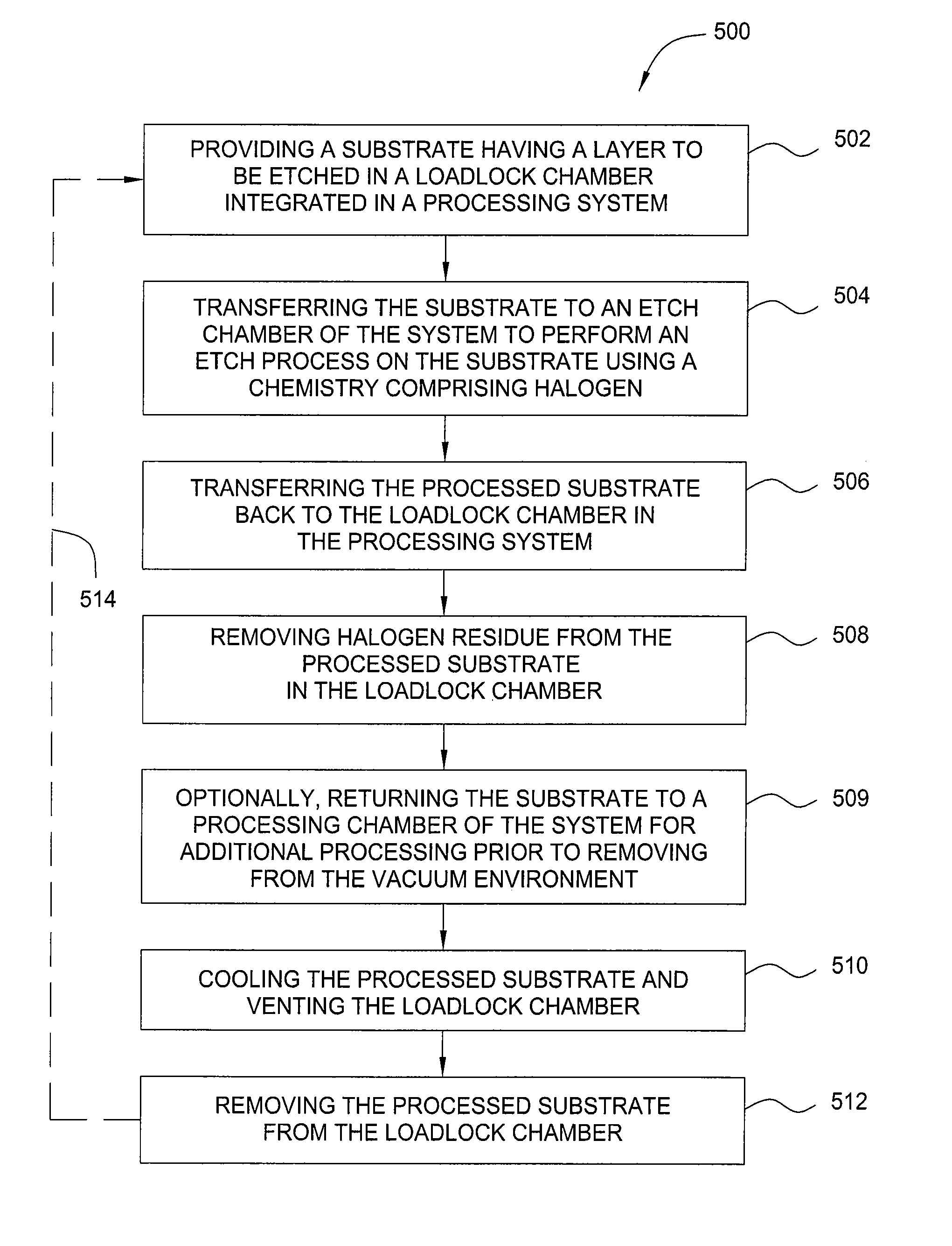
[0021]The present invention provides a method and apparatus for removing halogen-containing residues from a substrate etched using an etch ant that includes halogen. In one embodiment, the halogen-containing residues deposited during substrate etching are removed by a thermal treatment process performed in a load lock chamber integrated within a processing system. The load lock chamber heats the etched substrate and converts the halogen-containing residues into non-volatile compounds which may be pumped out of the load lock chamber. By performing the halogen-containing residue removal process in the load lock chamber during the substrate transfer sequence through the load lock chamber, the residue is removed without adversely increasing the overall process cycle time. The invention substantially prevents the environment of the processing system and the substrate from contamination and corrosion while maintaining high productivity and process throughput.

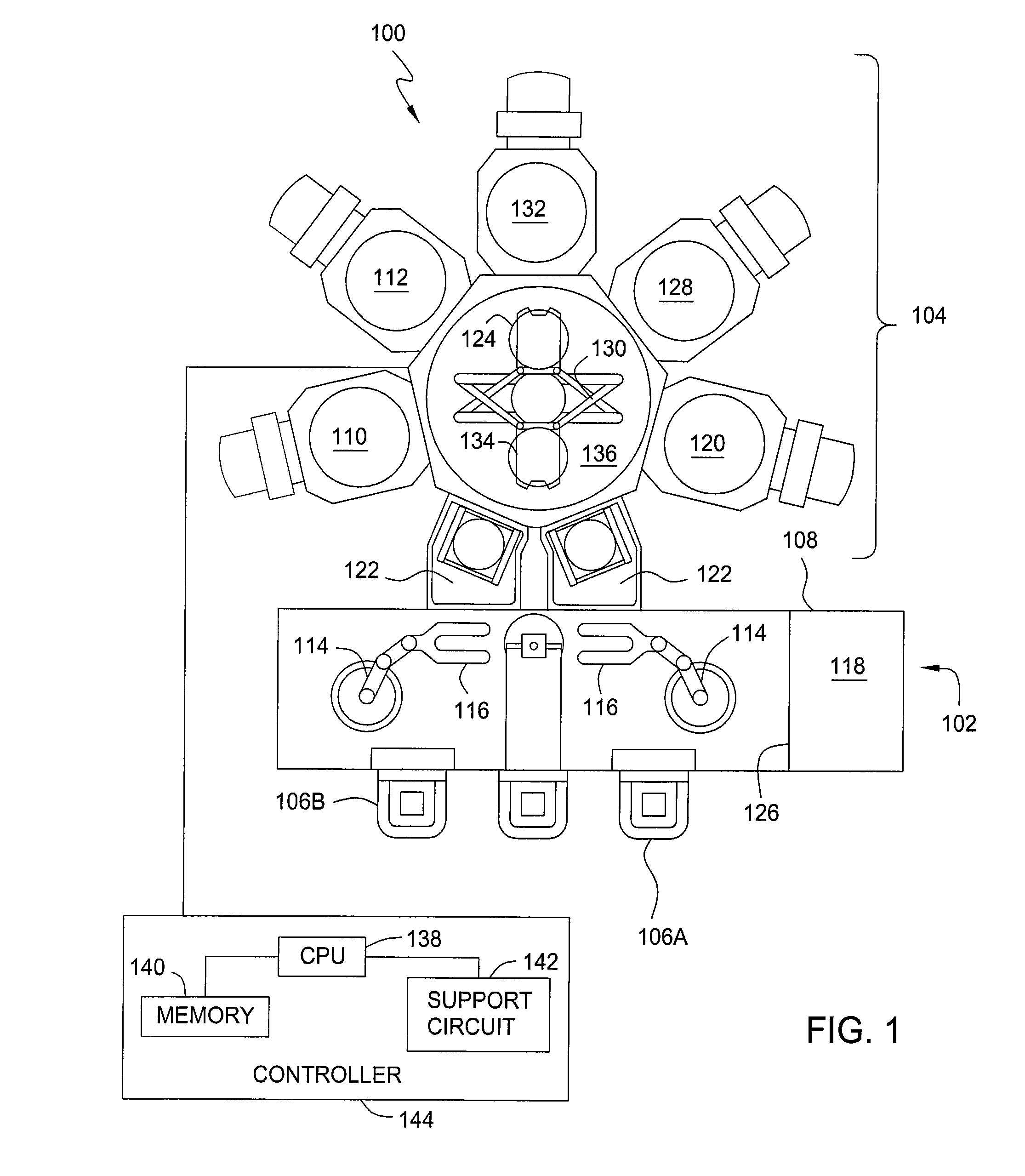
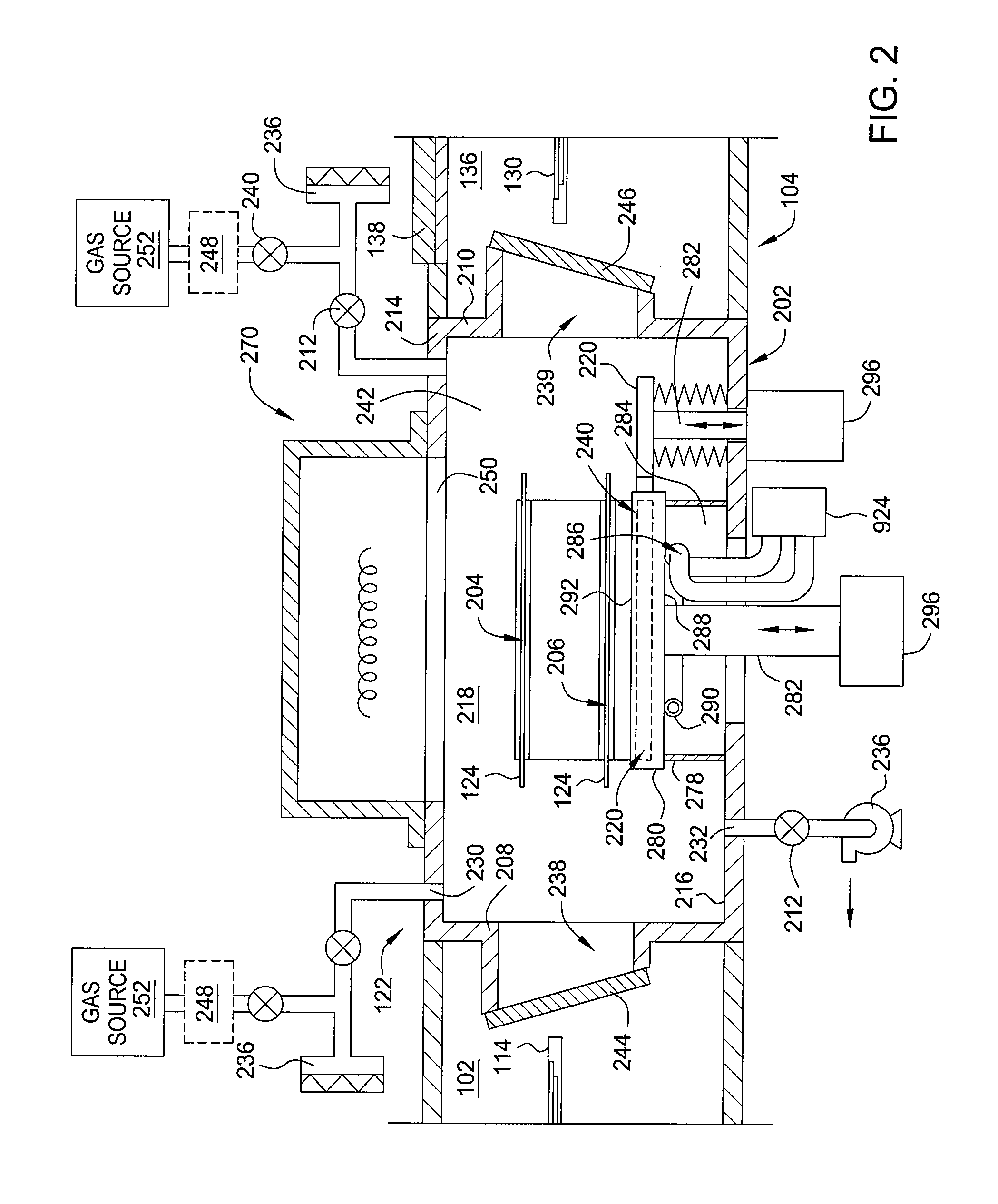
[0022]FIG. 1 is a schematic, t...


PUM

PropertyMeasurementUnit
temperatureaaaaaaaaaa
diameteraaaaaaaaaa

Abstract

A method and apparatus for removing volatile residues from a substrate are provided. In one embodiment, a method for volatile residues from a substrate includes providing a processing system having a load lock chamber and at least one processing chamber coupled to a transfer chamber, treating a substrate in the processing chamber with a chemistry comprising halogen, and removing volatile residues from the treated substrate in the load lock chamber.

Description

CROSS REFERENCE TO RELATED APPLICATIONS[0001]This application is a divisional of U.S. patent application Ser. No. 11 / 553,132, filed Oct. 26, 2006 (APPM / 10990), which is incorporated by reference in its entirety.BACKGROUND OF THE INVENTION[0002]1. Field of the Invention[0003]The present invention generally relates to a method and apparatus for fabricating devices on a semiconductor substrate. More specifically, the present invention relates to a method and apparatus for removing halogen-containing residues after plasma etching a layer on a semiconductor substrate.[0004]2. Description of the Related Art[0005]Ultra-large-scale integrated (ULSI) circuits may include more than one million electronic devices (e.g., transistors) that are formed on a semiconductor substrate, such as a silicon (Si) substrate, and cooperate to perform various functions within the device. Typically, the transistors used in the ULSI circuits are complementary metal-oxide-semiconductor (CMOS) field effect transi...

Claims


Application Information

Patent Timeline
Patent Type & Authority Applications(United States)
IPC IPC(8): C23C14/00
CPCH01L21/02057H01L21/02071H01L21/68742H01L21/67126H01L21/67201H01L21/67115
Inventor KAWAGUCHI, MARK NAOSHILO, KIN PONGHOOGENSEN, BRETT CHRISTIANWEN, SANDY M.KIM, STEVEN H.
Owner APPLIED MATERIALS INC
Why Eureka
Try Eureka