
Germanium oxide pre-clean module and process

a technology of germinium oxide and pre-cleaning module, which is applied in the field of pre-cleaning methods and apparatuses for a substrate surface, can solve the problems of affecting the electrical performance of the desired material layer, increasing the number of defects, and interfering with the formation of a desired material layer over the substrate surfa

Active Publication Date: 2016-10-18
ASM IP HLDG BV
View PDF80 Cites 262 Cited by
  • Summary
  • Abstract
  • Description
  • Claims
  • Application Information

AI Technical Summary

Benefits of technology

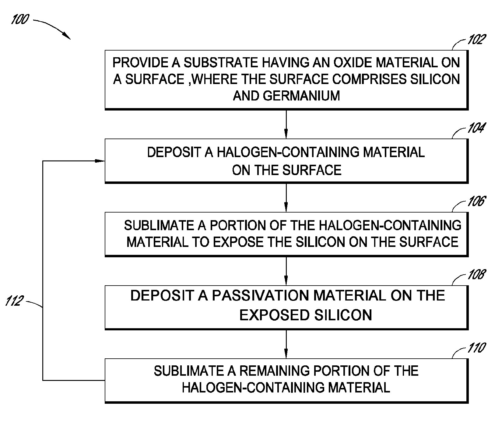
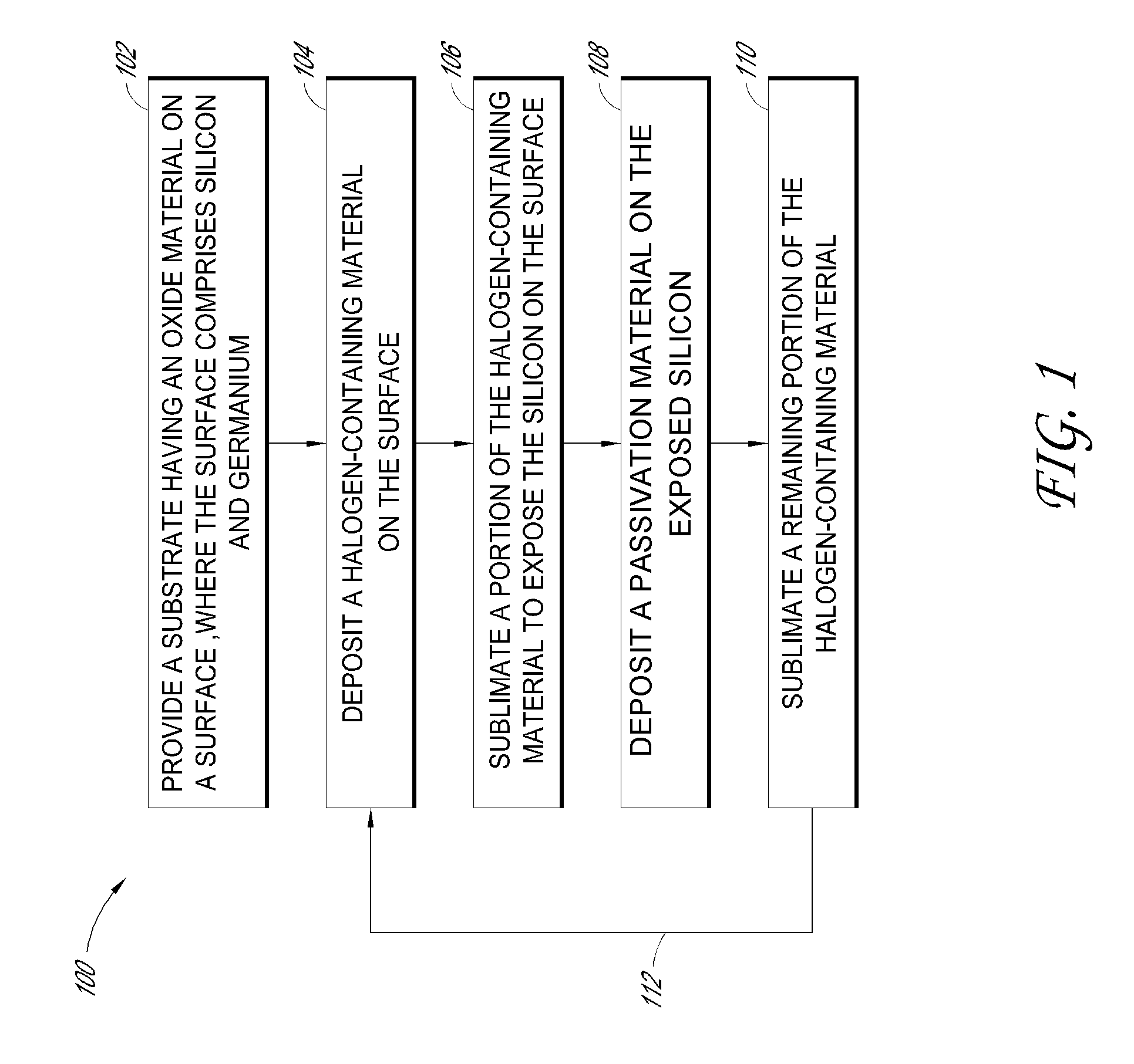
This patent describes a method for making integrated circuits by removing oxide material from certain surfaces. The method involves depositing a halogen-containing material on the surface and sublimating it to expose silicon or germanium. A passivation material containing chlorine is then deposited on the exposed silicon or germanium. This method allows for improved cleaning and passivation of the substrate surfaces, which can improve the performance and reliability of the integrated circuits.

Problems solved by technology

The presence of an intervening material (e.g., a native oxide layer, such as an oxide material layer comprising silicon and germanium on a silicon-germanium substrate) on the substrate surface may interfere with formation of a desired material layer over that substrate surface.
For example, the intervening material may cause introduction of an increased number of defects in the structure of the desired material layer and / or may adversely affect an electrical performance of the desired material layer.

Method used


Image

  • Germanium oxide pre-clean module and process
  • Germanium oxide pre-clean module and process
  • Germanium oxide pre-clean module and process

Examples


Embodiment Construction

[0015]Various embodiments are described herein in relation to a pre-cleaning process for removing oxide material from an exposed surface of a substrate. It will be understood that the resulting pre-cleaned surface can provide a surface that facilitates the later formation of high quality layers of materials, such as the epitaxial growth of silicon.

[0016]In some embodiments, a substrate pre-clean process is configured to remove an oxide material from the surface of a substrate comprising germanium, including substrate surfaces comprising germanium or both silicon and germanium. In some embodiments, the substrate surface can comprise both silicon and germanium at any molar ratio (e.g., Si1-xGex, where x greater than 0 and less than 1). For example, the process may remove a native oxide material from a silicon-germanium substrate. The pre-clean process can include depositing a pre-clean material on the substrate surface and subsequently volatizing the pre-clean material, thereby removi...


PUM

PropertyMeasurementUnit
temperatureaaaaaaaaaa
pressureaaaaaaaaaa

Abstract

In some embodiments, a method for integrated circuit fabrication includes removing oxide material from a surface of a substrate, where the surface includes silicon and germanium. Removing the oxide material includes depositing a halogen-containing pre-clean material on a silicon oxide-containing surface and sublimating a portion of the halogen-containing pre-clean material to expose the silicon on the surface. A passivation film is deposited on the exposed silicon. The passivation film may include chlorine. The passivation film may prevent contamination of the silicon surface by chemical species from the later sublimation, which may be at a higher temperature than the earlier sublimation. Subsequently, a remaining portion of the halogen-containing pre-clean material and the passivation film are sublimated. A target material, such as a conductive material, may subsequently be deposited on the substrate surface.

Description

BACKGROUND[0001]1. Field[0002]The present invention relates to the fabrication of integrated circuits, particularly to methods and apparatuses for pre-cleaning a substrate surface.[0003]2. Description of the Related Art[0004]Fabrication of integrated circuits often can involve formation of one or more material layers on a substrate surface. These material layers can include, for example, mono-crystalline, polycrystalline, and / or amorphous material layers. Formation of the material layers can be achieved using various thin film deposition techniques, including various physical (e.g., physical sputtering) and / or chemical (e.g., chemical vapor deposition, atomic layer deposition, and / or epitaxial deposition) deposition techniques. For example, mono-crystalline material formation on a substrate surface can be performed using an epitaxial deposition process, such as for formation of mono-crystalline semiconductor materials (e.g., mono-crystalline silicon).[0005]The presence of an interve...

Claims


Application Information

Patent Timeline
Patent Type & Authority Patents(United States)
IPC IPC(8): B05D3/02B05D3/04H05K3/00H01L21/306H01L21/02B05D3/00
CPCH05K3/0085H01L21/0206H01L21/02041H01L21/306B05D3/002B05D3/02B05D3/04B05D3/0433H01L21/02082H01L21/02096H01L21/02046
Inventor TOLLE, JOHNGOODMAN, MATTHEW G.
Owner ASM IP HLDG BV
Learn More