Method of Depositing Dielectric Film by ALD Using Precursor Containing Silicon, Hydrocarbon, and Halogen

Active Publication Date: 2012-11-22
ASM JAPAN
View PDF0 Cites 260 Cited by
  • Summary
  • Abstract
  • Description
  • Claims
  • Application Information

AI Technical Summary

Benefits of technology

[0013]By using the above precursors, replacement reaction such as carbonization and nitridation can substantially be improved, thereby enabling the formation of a film having desired components without substantial contamination and having high conformality (e.g., at least about 90%, or at least about 95%) even for an irregular surface having an aspect rat

Problems solved by technology

While the SiO process involving oxidizing replacement is basically insensitive to effects of temperature, etc., and thus can be performed at relatively low temperatures to form film, the SiN process requires high temperatures for film to be formed because nitriding replacement doe

Method used


Image

  • Method of Depositing Dielectric Film by ALD Using Precursor Containing Silicon, Hydrocarbon, and Halogen
  • Method of Depositing Dielectric Film by ALD Using Precursor Containing Silicon, Hydrocarbon, and Halogen
  • Method of Depositing Dielectric Film by ALD Using Precursor Containing Silicon, Hydrocarbon, and Halogen

Examples


example

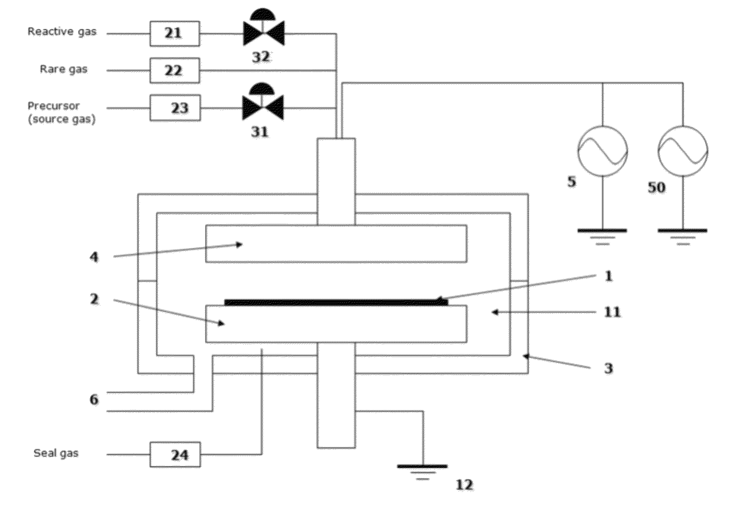
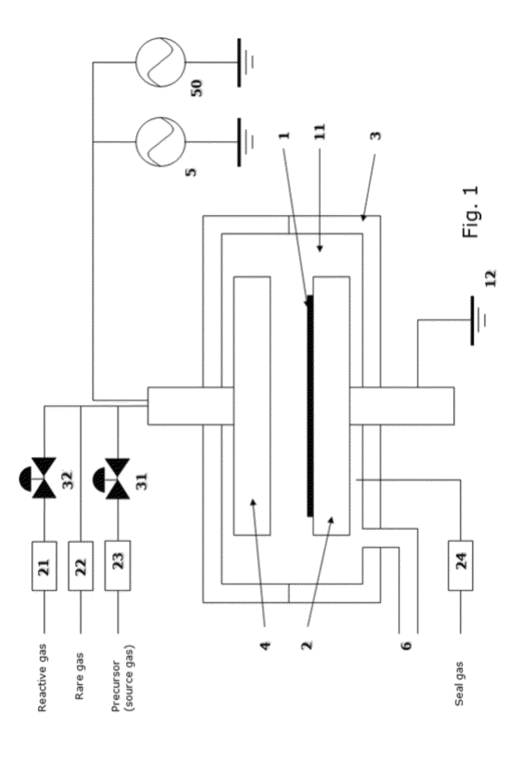
[0108]A dielectric film was formed on a 300-mm substrate having a patterned surface having an aspect ratio of about 2 and an opening width of about 50 nm under the condition shown below using Sequences 5 and 2 illustrated in FIGS. 6 to 7 and the PEALD apparatus illustrated in FIG. 1 with a modification using the flow switching control system illustrated in FIG. 5. The thickness of film was 30 nm for evaluating film properties. The conditions for depositing a film were as follows and are also shown in Table 1.

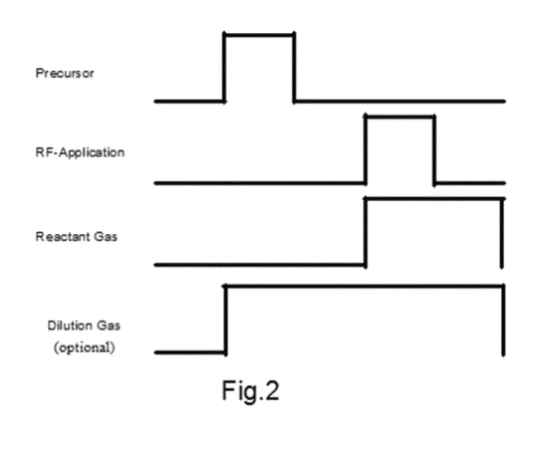
[0109]Sequence 5 (FIG. 6)—Comparative Example:[0110]Precursor inflow pressure: 133-1333 Pa (It depended on vapor pressure of precursor)[0111]Carrier gas (Ar) flow: 2000 sccm[0112]RF frequency: 13.56 MHz[0113]Precursor supply time (“Feed”): 0.1-1 sec supply (It depended on vapor pressure of precursor)[0114]Purge time after precursor pulse (“Purge”): 1 sec[0115]Reactant gas supply time: continuous[0116]Purge time after reactant gas pulse (“Purge”): 1 sec[0117]RF Plasma exciting ti...


PUM

PropertyMeasurementUnit
Temperatureaaaaaaaaaa
Timeaaaaaaaaaa
Timeaaaaaaaaaa

Abstract

A method of forming a dielectric film having at least Si—N, Si—C, or Si—B bonds on a semiconductor substrate by atomic layer deposition (ALD), includes: supplying a precursor in a pulse to adsorb the precursor on a surface of a substrate; supplying a reactant gas in a pulse over the surface without overlapping the supply of the precursor; reacting the precursor and the reactant gas on the surface; and repeating the above steps to form a dielectric film having at least Si—N, Si—C, or Si—B bonds on the substrate. The precursor has at least one Si—C or Si—N bond, at least one hydrocarbon, and at least two halogens attached to silicon in its molecule.

Description

CROSS-REFERENCE TO RELATED APPLICATIONS [0001]This application is a continuation-in-part of U.S. patent application Ser. No. 13 / 030,438, filed Feb. 18, 2011, the disclosure of which is herein incorporated by reference in its entirety. The applicant(s) herein explicitly rescind(s) and retract(s) any prior disclaimers or disavowals made in any parent, child or related prosecution history with regard to any subject matter supported by the present application.BACKGROUND [0002]1. Field of the Invention[0003]The present invention relates generally to semiconductor integrated circuit manufacturing and, more particularly to a method of forming a dielectric film having at least Si—N, Si—C, or Si—B bonds on a semiconductor substrate by atomic layer deposition (ALD).[0004]2. Description of the Related Art[0005]SiC, SiCN, SiCO and other silicon carbide insulation films were adopted as etching stopper films and Cu diffusion blocking films for devices installed with Cu wirings. These films provid...

Claims


Application Information

Patent Timeline
IPC IPC(8): H01L21/314H01L21/318
CPCC23C16/30C23C16/45553H01L21/02167C23C16/45542H01L21/02211H01L21/02274H01L21/0228H01L21/0217
Inventor FUKAZAWA, ATSUKI
Owner ASM JAPAN
Why Eureka
Try Eureka