Image Forming Device and Control Method Thereof

a technology of forming device and image, which is applied in the direction of electrographic process apparatus, optics, instruments, etc., can solve the problems of affecting damage to the protective layer on the surface of the photoconductor or even the photoconductor layer, and inability to print correctly, so as to improve the cleanability of the latent image carrier, improve the cleanability, and facilitate the recovery of the developer

Inactive Publication Date: 2009-01-15
SEIKO EPSON CORP
View PDF5 Cites 6 Cited by
  • Summary
  • Abstract
  • Description
  • Claims
  • Application Information

AI Technical Summary

Benefits of technology

[0017]Further, the latent image carrier cleaning roller applies the bias with the same polarity as the polarity of the bias applied to the transfer bias applying section when the image on the latent image carrier is transferred. Therefore, it becomes easy to recover the developer by the latent image carrier cleaning roller, thus the cleanability can be improved.
[0018]Further, a transfer member having a transfer bias applying section for applying a bias for transferring the image on the latent image carrier is provided, and the cleaning process control section executes the cleaning process while the transfer member has contact with the latent image carrier. Therefore, the developer on the latent image carrier is transferred to the transfer member, and thus the cleanability of the latent image carrier can be improved.
[0019]Further, the latent image carrier cleaning roller applies the bias with the reverse polarity from the polarity of the bias applied to the transfer bias applying section when the image on the latent image carrier is transferred. Therefore, the developer regularly charged is transferred to the transfer member while the developer not regularly charged is recovered by the latent image carrier cleaning roller, thus the cleanability can be improved.
[0020]Further, a squeezing member for recovering a carrier liquid on the latent image carrier is provided, and the cleaning process control section separates the squeezing member therefrom. Therefore, the recovery of the carrier liquid is reduced, thus it becomes easy to scrape out the developer with the latent image carrier cleaning blade or the like.
[0021]Further, the squeezing member includes a first squeezing roller and a second squeezing roller. Therefore, the carrier liquid can sufficiently be removed in the printing state, thus the image quality can be improved.

Problems solved by technology

However, in the case of cleaning the photoconductor, in contrast with cleaning of the intermediate transfer belt, if compact clusters of the toner particles or the toner particles still remain after slipping through a cleaning blade, the toner particles are charged by the friction between the cleaning blade and the toner particles, and further, by discharging electricity from the toner particles thus charged to the photoconductor, a protective layer on the surface of the photoconductor or even the photoconductor layer, in some cases, might be damaged.
The photoconductor in such a condition can hardly be charged normally, and problematically causes faulty printing.
Further, if the photoconductor surface is contaminated by faulty cleaning, when an electric latent image is formed on the surface of the photoconductor by an exposure device, there is caused a problem that the exposure light is diffused to disturb the latent image or a problem that the electric latent image formed of the surface of the photoconductor can hardly be maintained.
Further, in the case in which the toner particles remains on the surface of the photoconductor as disclosed in Document 2, since the toner particles remaining on the photoconductor form compact clusters, it becomes further difficult to remove them by cleaning with a normal cleaning blade, and accordingly, such toner particles forming the compact clusters cannot be cleaned but slip through the cleaning blade to cause the problem of damaging the surface of the photoconductor.

Method used


Image

  • Image Forming Device and Control Method Thereof
  • Image Forming Device and Control Method Thereof
  • Image Forming Device and Control Method Thereof

Examples


first embodiment

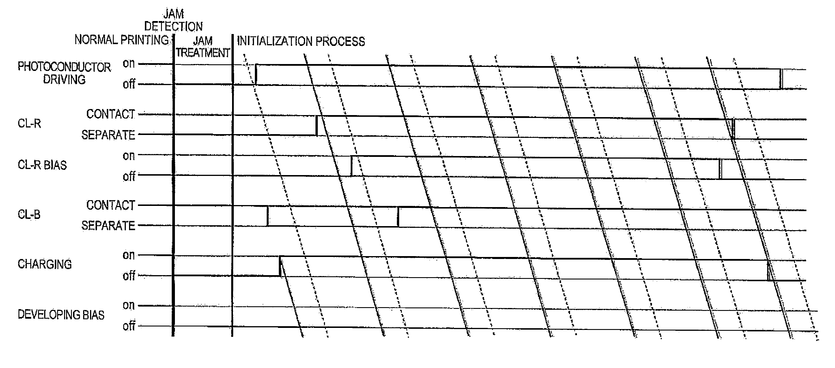
[0063]FIG. 5 shows a timing chart of the photoconductor cleaning control. It should be noted that solid slant lines each represent a front edge position of the charged area, and dotted slant lines each represent a front edge position of the toner not yet transferred.

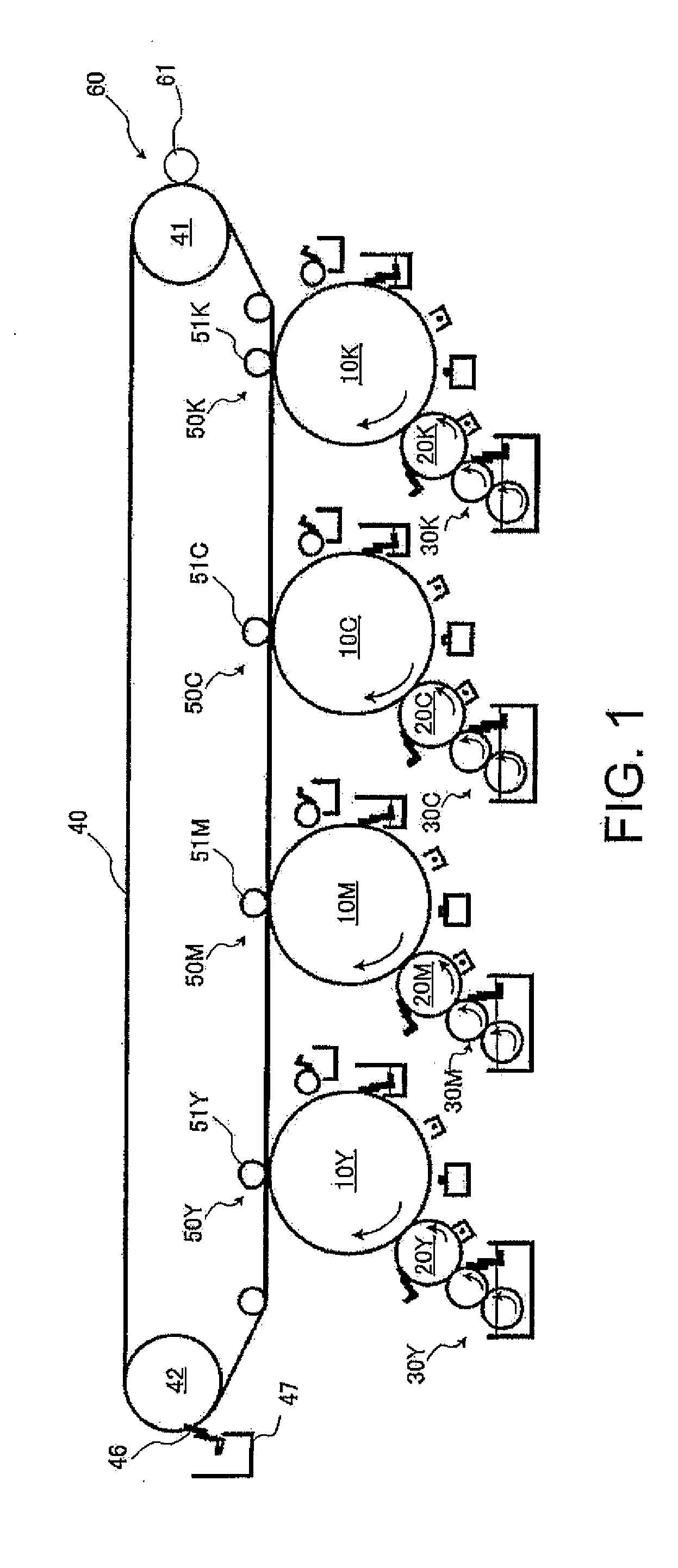
[0064]Firstly, in a printing state, as shown in FIG. 2, the photoconductor 10Y is driven, a charging bias of about +600 V and a developing bias of about +400 V are both applied in ON states, the photoconductor cleaning roller 82Y is separated with no bias applied, namely with the bias in an OFF state, and the photoconductor cleaning blade 87Y is contacted thereto.

[0065]In this condition, the liquid developer supplied from the agitating supplying roller 34Y to the developer supply roller 32Y is regulated by the regulating blade 33Y to be in a condition in which the amount of developer is adjusted, and then the liquid developer is transferred to the developing roller 20Y, and further to the portions of the photoconductor 1...

fourth embodiment

[0100]FIG. 15 shows a timing chart of the photoconductor cleaning process control.

[0101]It should be noted that solid slant lines each represent a front edge position of the charged area, and dotted slant lines each represent a front edge position of the toner not yet transferred.

[0102]Firstly, in a printing state, the photoconductor 10Y is driven, a charging bias of about +600 V and a developing bias of about +400 V are both applied in ON states, the photoconductor cleaning roller 82Y is not applied with the bias in the OFF state, and the photoconductor cleaning blade 87Y is contacted thereto.

[0103]In this condition, the liquid developer supplied from the agitating supplying roller 34Y to the developer supply roller 32Y is regulated by the regulating blade 33Y to be in a condition in which the amount of developer is adjusted, and then the liquid developer is transferred to the developing roller 20Y, and further to the portions of the photoconductor 10Y on which the latent image is ...


PUM


Abstract

An image forming device includes a developer carrier for carrying a liquid developer, a latent image carrier to which a latent image is developed by the developer carrier, a charging member for charging the latent image carrier, an exposure device for exposing the latent image carrier, a latent image carrier cleaning roller for applying a bias to clean the latent image carrier, a latent image carrier cleaning blade having contact with the latent image carrier and for scraping out the developer on the latent image carrier, and a cleaning process control section for cleaning the latent image carrier in a condition in which a charging bias of the charging member is applied, the developer carrier has contact with the latent image carrier, and the bias of the latent image carrier cleaning roller is applied to the latent image carrier cleaning roller.

Description

CROSS REFERENCE TO RELATED APPLICATION[0001]The disclosure of Japanese Patent Applications No. 2007-184016 filed on Jul. 13, 2007 and No. 2008-12233 filed on Jan. 23, 2008 including specification, drawings and claims is incorporated herein by reference in its entirety.BACKGROUND[0002]1. Technical Field[0003]The present invention relates to an image forming device using a liquid developer having toner dispersed in a carrier liquid, and a control method of the image forming device.[0004]2. Related Art[0005]A developer used for a wet image forming device has toner particles mixed in an electrical insulating organic solvent, and since the particle diameter of the toner particles is as extremely fine as 2 μm or smaller (typically 1 μm or smaller), which can achieve higher image quality in comparison with a dry image forming device using toner powder with a size of about 7 μm. At the same time, since the toner particles are small, cleanability is lowered.[0006]Therefore, in the past, ther...

Claims


Application Information

Patent Timeline
Patent Type & Authority Applications(United States)
IPC IPC(8): G03G15/00G03G21/00
CPCG03G15/10G03G2221/0005G03G21/0058
Inventor CHIBA, SATOSHIIKUMA, KEN
Owner SEIKO EPSON CORP
Why Eureka
Try Eureka