Nonvolatile memory device and method of operating fabricating the same

a nonvolatile memory and fabrication method technology, applied in semiconductor devices, digital storage, instruments, etc., can solve the problems of reducing the reliability of the tunneling insulating layer, more difficult to erase data by applying a body bias to the substrate, etc., and achieve the effect of reliable operation

Inactive Publication Date: 2009-01-22
SAMSUNG ELECTRONICS CO LTD
View PDF6 Cites 50 Cited by
  • Summary
  • Abstract
  • Description
  • Claims
  • Application Information

AI Technical Summary

Benefits of technology

[0005]Example embodiments provide a method of more reliably operating a more highly integratable nonvolatile memory device.

Problems solved by technology

Thus, in three-dimensional nonvolatile memory devices, it may be more difficult to erase data by applying a body bias to a substrate, unlike in conventional two-dimensional nonvolatile memory devices.
However, this may lower the reliability of a tunneling insulating layer.

Method used


Image

  • Nonvolatile memory device and method of operating fabricating the same
  • Nonvolatile memory device and method of operating fabricating the same
  • Nonvolatile memory device and method of operating fabricating the same

Examples


Embodiment Construction

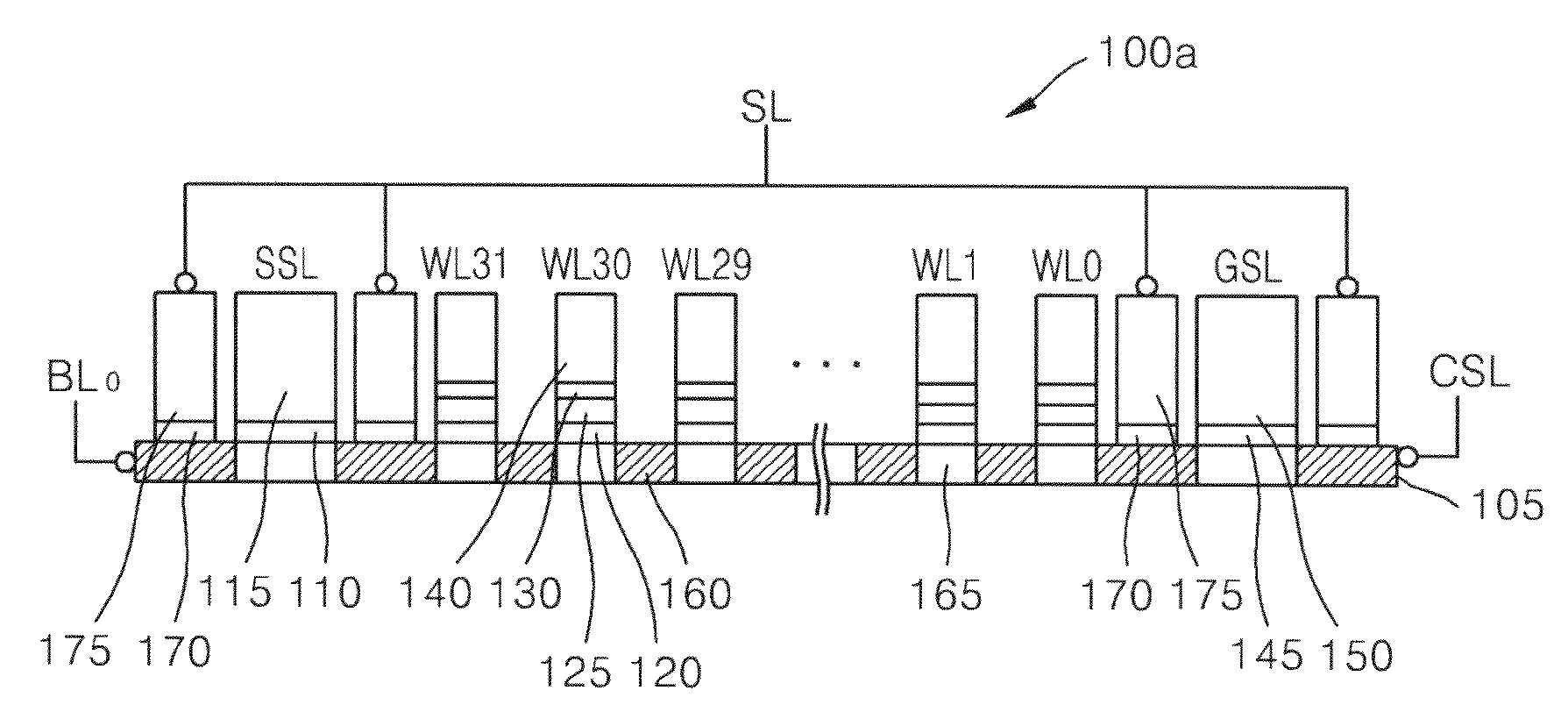
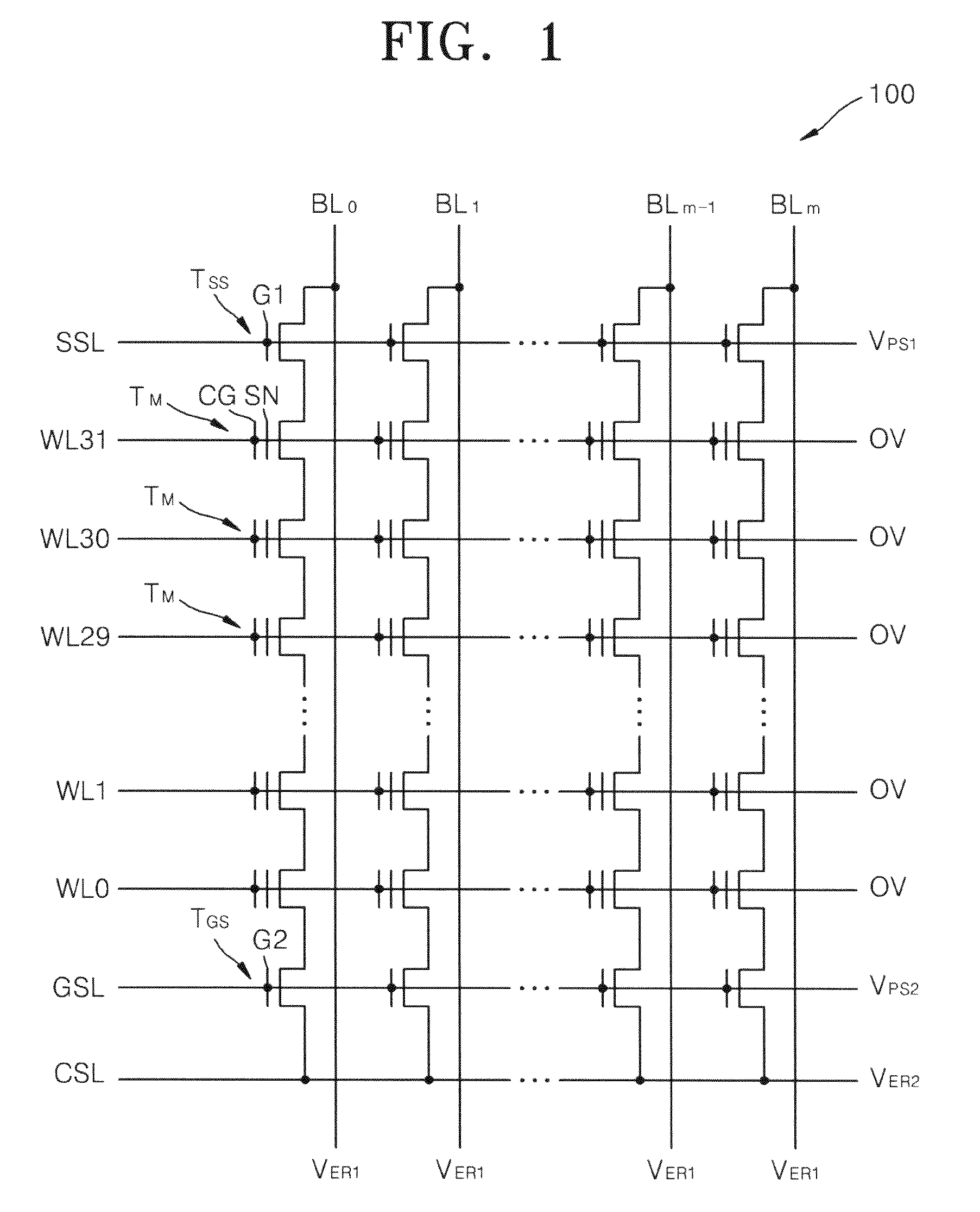
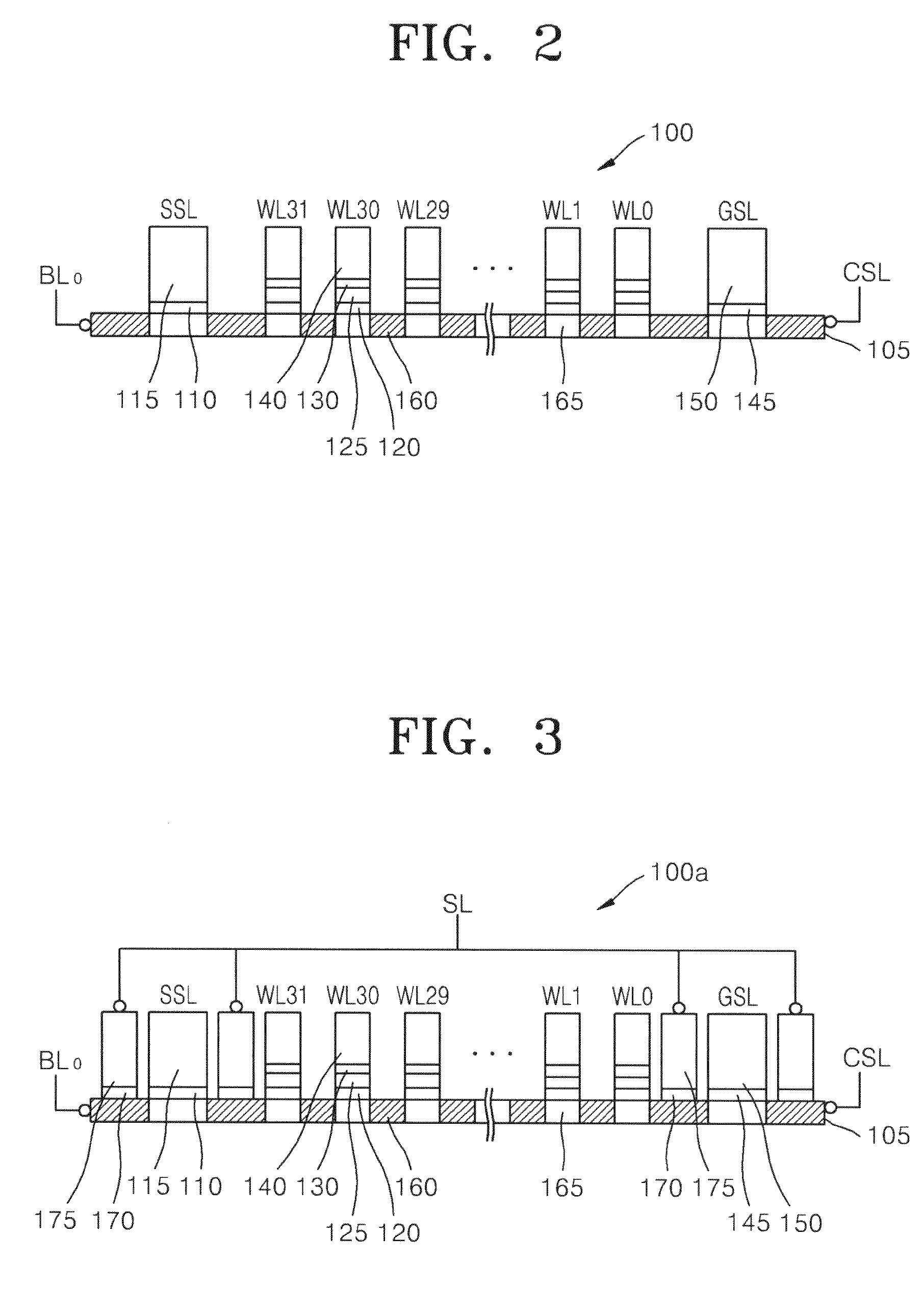
[0022]Example embodiments will now be described more fully with reference to the accompanying drawings, in which example embodiments are shown. Example embodiments may, however, be embodied in many different forms and should not be construed as being limited to the example embodiments set forth herein. Rather, example embodiments are provided so that this disclosure will be thorough and complete, and will fully convey the scope of the invention to one of ordinary skill in the art. In the drawings, the sizes of constitutional elements may be exaggerated for the convenience of illustration.

[0023]In example embodiments, rows and columns may be relatively designated according to a viewing direction. Thus, rows and columns may be interchanged.

[0024]Accordingly, while example embodiments are capable of various modifications and alternative forms, embodiments thereof are shown by way of example in the drawings and will herein be described in detail. It should be understood, however, that t...


PUM


Abstract

Provided is a method of reliably operating a highly integratable nonvolatile memory device. The nonvolatile memory device may include a string selection transistor, a plurality of memory transistors, and a ground selection transistor between a bit line and a common source line. In the nonvolatile memory device, data may be erased from the memory transistors by applying an erasing voltage to the bit line or the common source line.

Description

PRIORITY STATEMENT[0001]This application claims priority under 35 U.S.C. § 119 to Korean Patent Application No. 10-2007-0058573, filed on Jun. 14, 2007, in the Korean Intellectual Property Office, the disclosure of which is incorporated herein in its entirety by reference.BACKGROUND[0002]Nonvolatile memory devices, e.g., electronically erasable programmable read only memories (EEPROMs) or flash memories may store data even when power is turned off, and further, stored data may be erased therefrom and new data may be programmed thereto. Nonvolatile memory devices may be used in semiconductor products, e.g., storage media for mobile devices or portable memory sticks, etc.[0003]Recently, with the trend toward smaller semiconductor products, nonvolatile memory devices used in the semiconductor products have become more highly integrated. For example, three-dimensional nonvolatile memory devices may have a higher degree of integration in a plane compared to two-dimensional nonvolatile me...

Claims


Application Information

Patent Timeline
Patent Type & Authority Applications(United States)
IPC IPC(8): G11C16/06
CPCG11C16/16H01L27/11524H01L27/11521H01L27/115H10B41/35H10B69/00H10B41/30G11C16/0483G11C16/08G11C16/14G11C16/30
Inventor HONG, KI-HALEE, SUNG-HOONHYUN, JAE-WOONGSHIN, JAI-KWANGJIN, YOUNG-GUPARK, SUNG-ILKIM, JONG-SEOB
Owner SAMSUNG ELECTRONICS CO LTD
Why Eureka
Try Eureka