Hermetic pacakging and method of manufacture and use therefore

a technology of pacakging and pacakging, which is applied in the direction of chemistry apparatus and processes, semiconductor/solid-state device details, coatings, etc., can solve the problem of only suitable small-scale devices

Inactive Publication Date: 2009-01-29
WAN CHANG FENG
View PDF0 Cites 50 Cited by
  • Summary
  • Abstract
  • Description
  • Claims
  • Application Information

AI Technical Summary

Problems solved by technology

However, because of the permeability and possible out-gassing of the epoxy seals, the package is classified as non-hermetic.
This approach is only suitable for very small devices because the films are much thinner than the cap wafers made from bulk material.

Method used


Image

  • Hermetic pacakging and method of manufacture and use therefore
  • Hermetic pacakging and method of manufacture and use therefore
  • Hermetic pacakging and method of manufacture and use therefore

Examples


Embodiment Construction

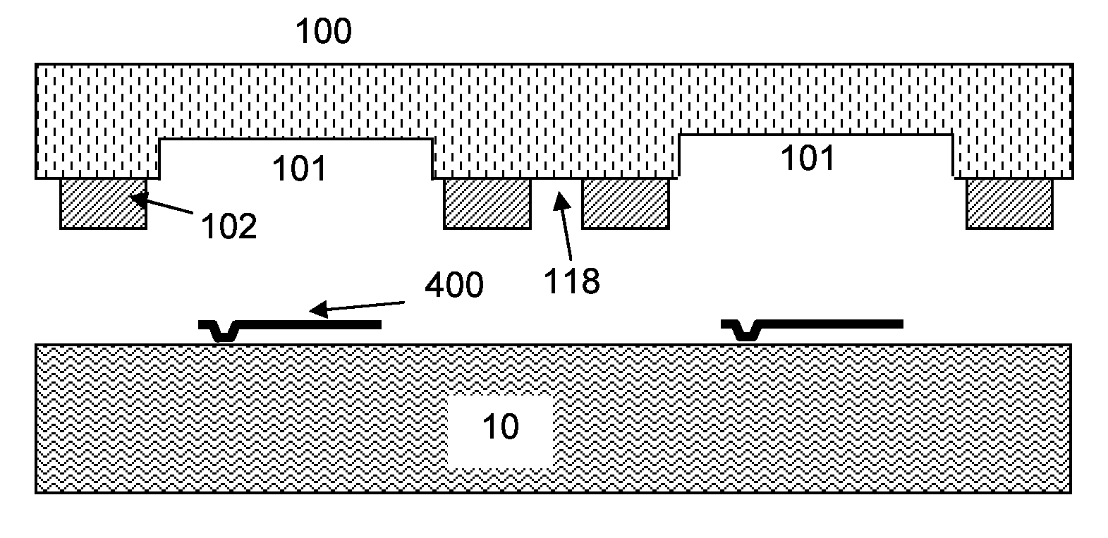
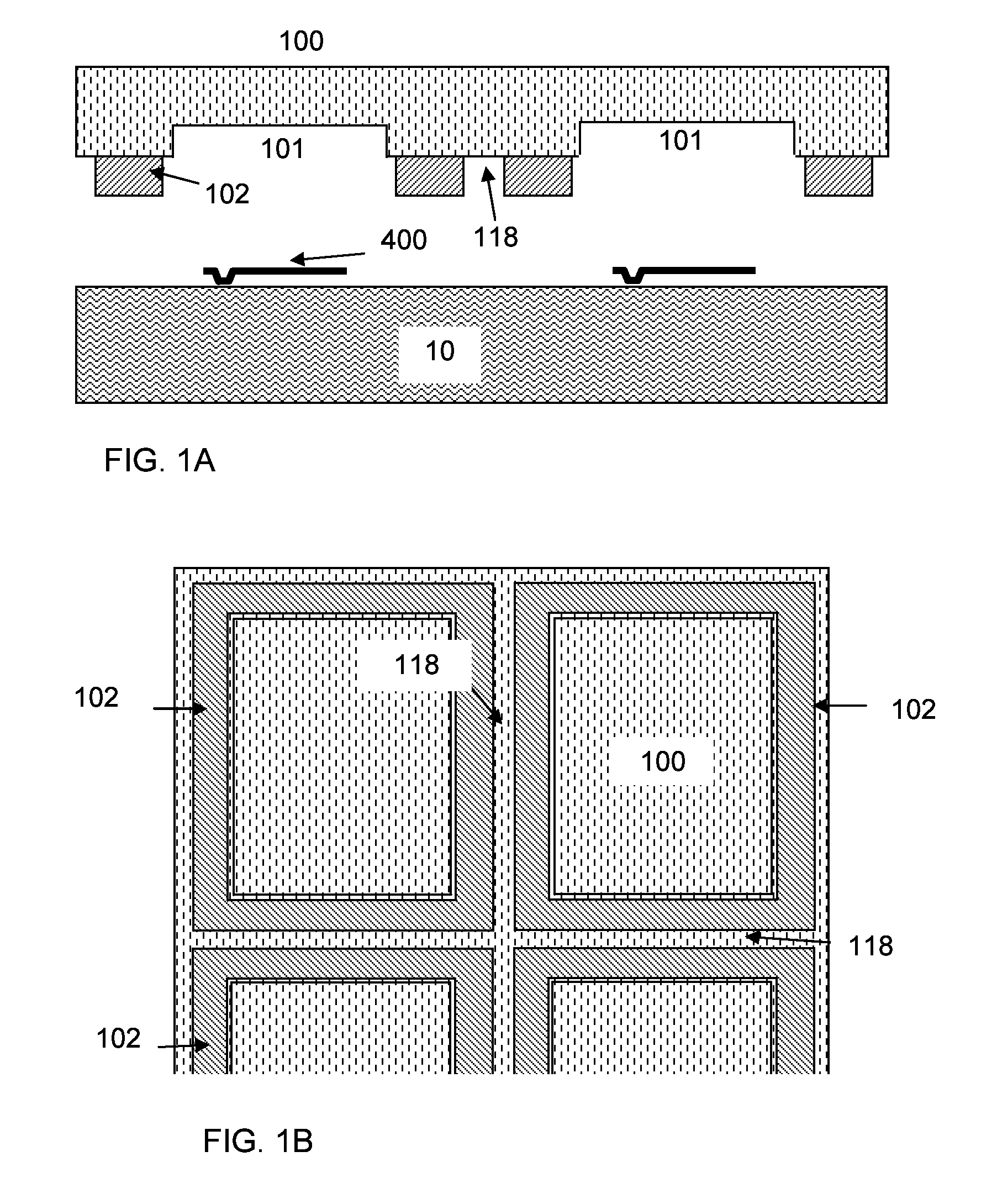
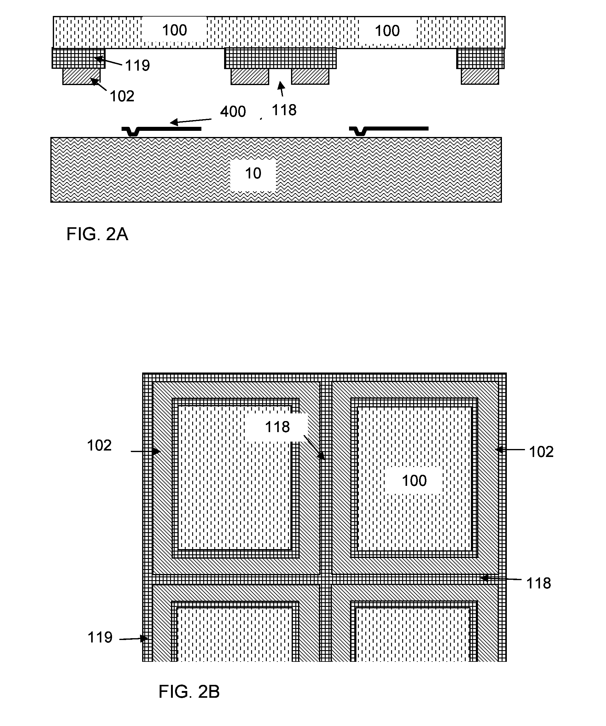
[0010]A method and system for cavity packaging MEMS devices, such as the DLP™ (digital light processor) on wafer scale in hermetic or vacuum seal is described herein. The processes of the wafer-level packaging begin during or after the final phase of the MEMS device fabrication process, and before the wafer are diced into separate chips. Referring now to FIGS. 1 to 9, there is a depicted cross-sectional view showing a particular portion of a microstructure during specific phases of the packaging process for the exemplary MEMS device. The dimensions are not shown to scale.

[0011]FIG. 1A depicts cross-sectional view of a microelectronics substrate 10, which comprises micromechanical structures 400, and a cap wafer 100. A plurality of adhesive rings 102, with gap 118 between them, are formed on the cap wafer 100, as shown in plain view of FIG. 1B. Alternatively the adhesive rings may be formed on the substrate wafer 10. The cap wafer 100 may have cavities 101 etched thereon and is prefe...


PUM

PropertyMeasurementUnit
widthaaaaaaaaaa
volumeaaaaaaaaaa
sizeaaaaaaaaaa

Abstract

An embodiment of the present invention provides a method of manufacturing hermetic packaging for devices on a substrate wafer, comprising forming a plurality of adhesive rings on a cap wafer or the substrate wafer, bonding the cap wafer to the substrate wafer with an adhesive layer, forming trenches in the cap wafer and the adhesive rings along outer rim of the adhesive rings, and covering sidewall of the trenches by at least one deposited film to provide a diffusion barrier to moisture or gas.

Description

CROSS-REFERENCE TO RELATED APPLICATIONS[0001]This application is a divisional of application Ser. No. 11 / 113,545, filed Apr. 25, 2005 claiming This claims the benefit of the following provisional patents: attorney's docket number JSF02-0009 filed Jun. 1, 2004 (APPL No. 60 / 575,586), attorney's docket number JSF02-0010 filed Sep. 7, 2004 (APPL No. 60 / 607,723), and attorney's docket number JSF02-0011 filed Nov. 8, 2004 entitled, “METHOD OF MANUFACTURING HERMETIC PACKAGING” (APPL NO TBD).BACKGROUND[0002]Hermetic packaging, which provides tightly sealed cavities, has been used to protect many MEMS (micorelectromechnaical systems), such as optical, RF (radio frequency) and sensor devices, against moisture and other corrosive gases from seeping in, or to keep under controlled atmosphere. Specific examples include DLP™, bolometer, accelerometers and gyroscope. Wafer-level packaging offers advantages for packaging of cavities brings the cost advantage of simultaneously sealing an entire wafe...

Claims


Application Information

Patent Timeline
Patent Type & Authority Applications(United States)
IPC IPC(8): H01L21/50B81C1/00H01L23/02H01L23/10
CPCY10T156/1052B81C1/00269H01L2924/16235
Inventor WAN, CHANG-FENG
Owner WAN CHANG FENG
Why Eureka
Try Eureka