Structure and method for detecting errors in a multilevel memory device with improved programming granularity

a multi-level memory and programming granularity technology, applied in the direction of error detection/correction, fault response, static storage, etc., can solve the problems of high density of multi-level memory devices, low cost per unit of stored information, and multi-level memory devices being considered more sensitive to data retention

Active Publication Date: 2009-02-12
VISCONTI ANGELO
View PDF5 Cites 7 Cited by
  • Summary
  • Abstract
  • Description
  • Claims
  • Application Information

AI Technical Summary

Problems solved by technology

This results in a high density of the multilevel memory device, with a consequent low cost per units of stored information.
In fact, the multilevel memory devices are considered more sensitive to data retention problems and to noise than equivalent traditional memory devices (at two levels).
Nevertheless, the error detection structures known in the art involve a considerable waste of space for storing the control information associated with the various pages.
Furthermore, the logic networks commonly used for calculating the control information require a high number of levels; such levels introduce corresponding propagation delays of the signals, thereby slowing down the operation of the whole multilevel memory device.
Furthermore, the error detection structures impose some constraints to the operation of the multilevel memory device.
Particularly, once a page with the respective control information has been written onto the multilevel memory device, it is generally impossible to modify its content any longer (without a complete erasing and re-writing of the updated page with the new control information).
Such requirements cannot be satisfied by the error detection structures known in the art.
In fact, this would require an amount of control information that is absolutely unacceptable, thereby making vain the advantages provided by the use of three multilevel memory devices.

Method used


Image

  • Structure and method for detecting errors in a multilevel memory device with improved programming granularity
  • Structure and method for detecting errors in a multilevel memory device with improved programming granularity
  • Structure and method for detecting errors in a multilevel memory device with improved programming granularity

Examples


Embodiment Construction

[0017]The following discussion is presented to enable a person skilled in the art to make and use the invention. Various modifications to the embodiments will be readily apparent to those skilled in the art, and the generic principles herein may be applied to other embodiments and applications without departing from the spirit and scope of the present invention. Thus, the present invention is not intended to be limited to the embodiments shown, but is to be accorded the widest scope consistent with the principles and features disclosed herein.

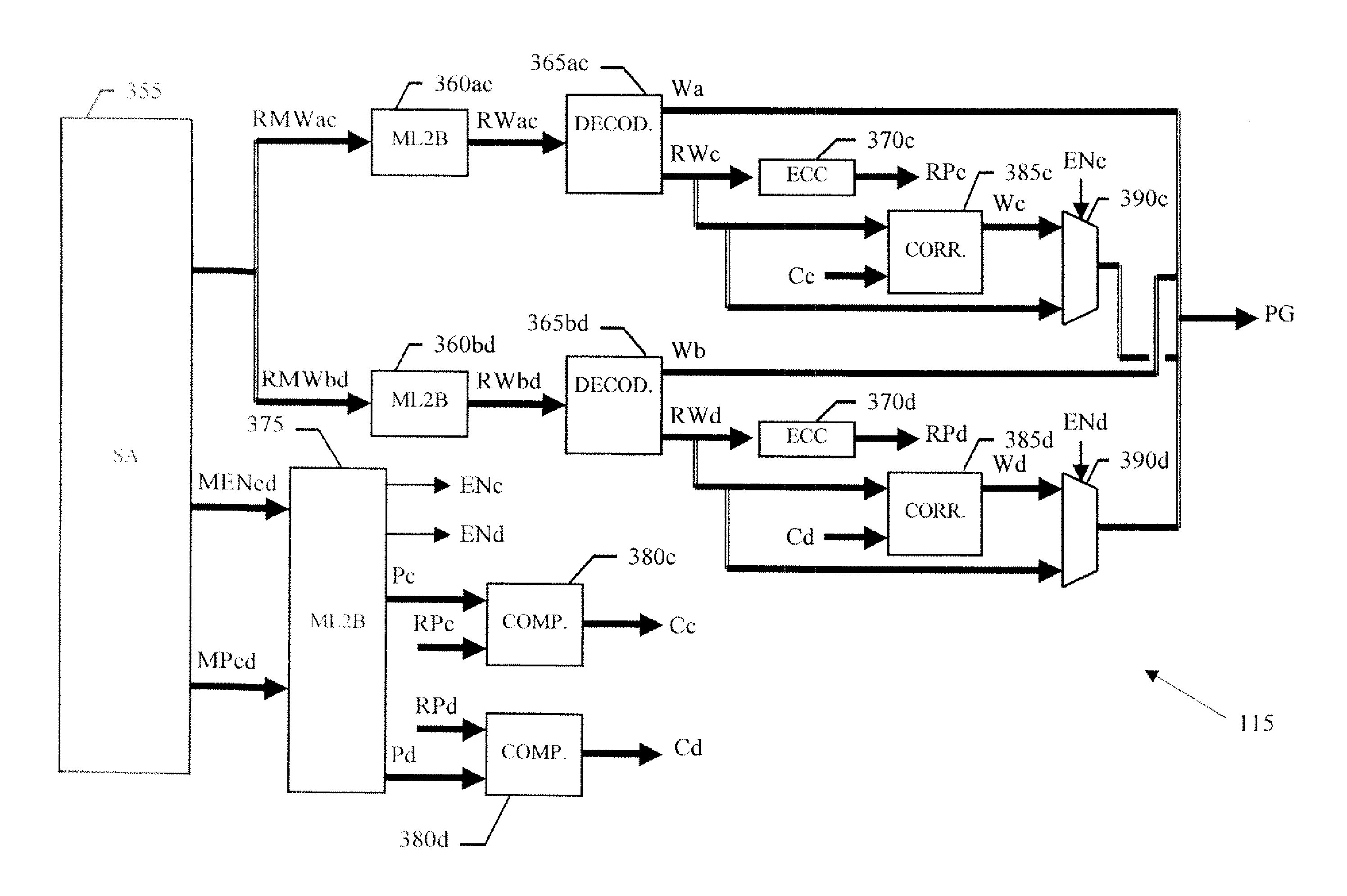
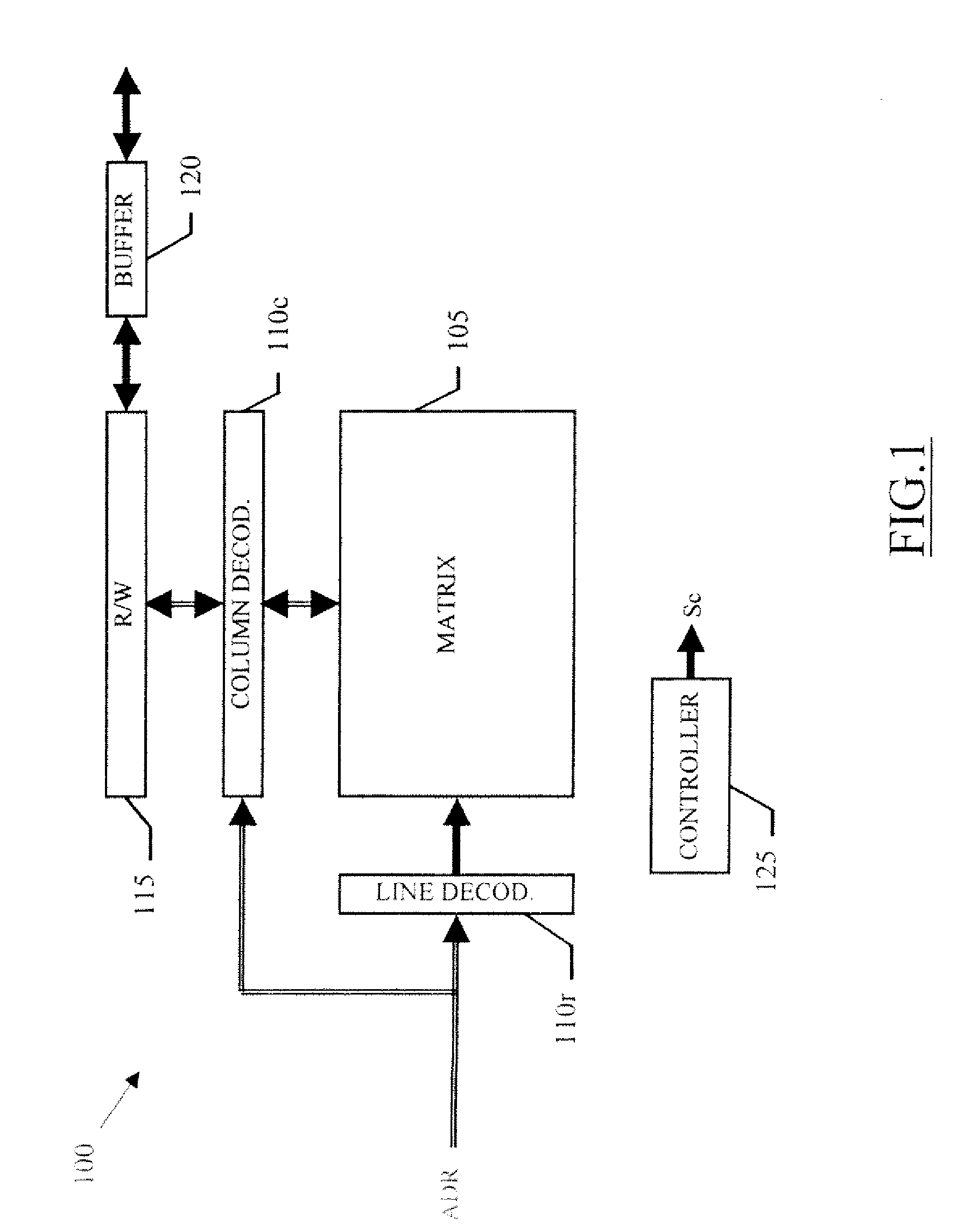
[0018]With reference in particular to FIG. 1, a non-volatile memory device 100, for example, consisting of a flash E2PROM, is illustrated. The flash memory 100 is integrated on a chip of semiconductor material, and includes a matrix 105 of memory cells (for example, having a so-called NOR architecture).

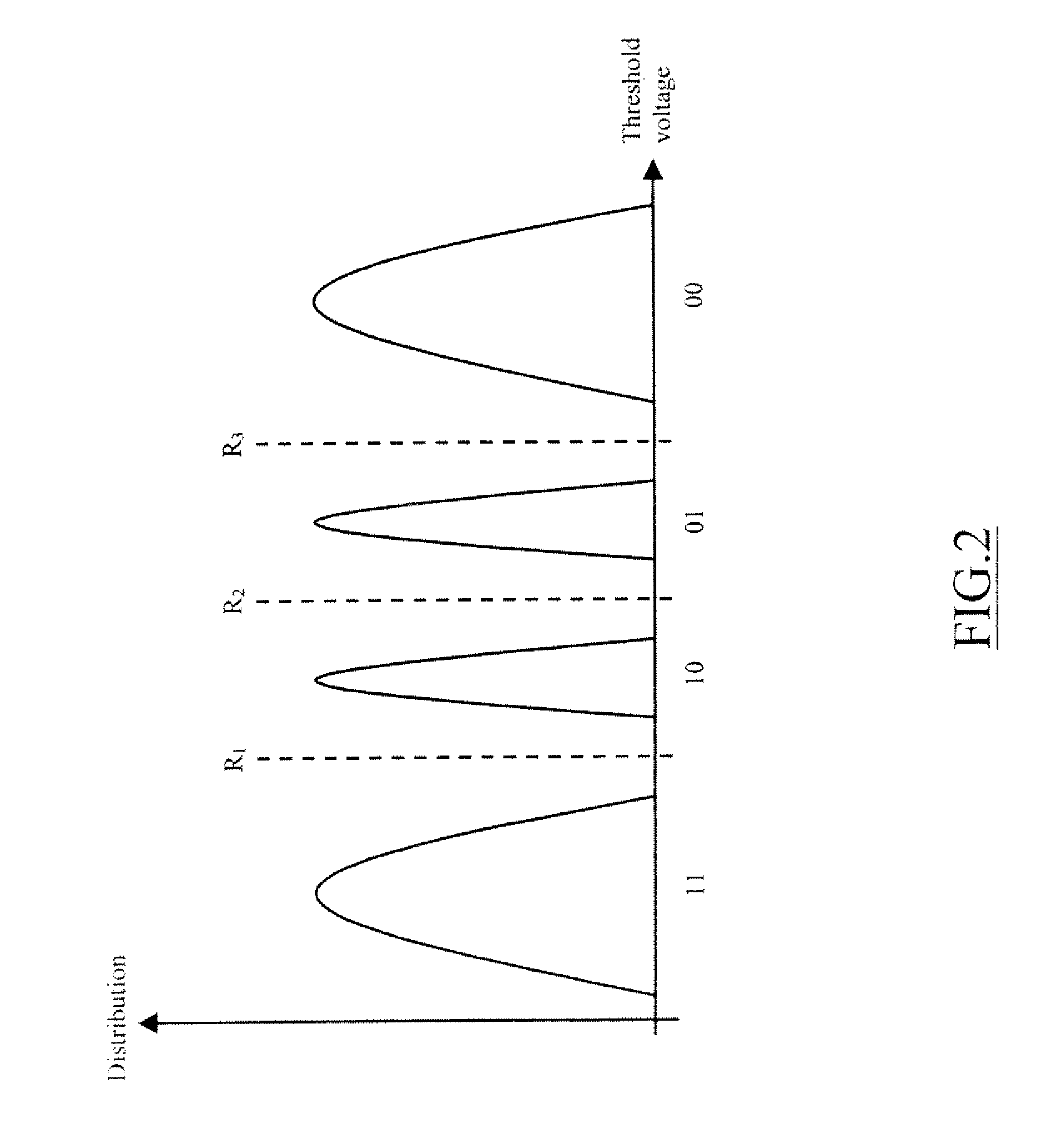
[0019]Each memory cell consists of a floating gate MOS transistor. The memory cell in a non-programmed (or erased) condition exhibits a low thre...


PUM


Abstract

An error detection structure is proposed for a multilevel memory device including a plurality of memory cells each one being programmable at more than two levels ordered in a sequence, each level representing a logic value consisting of a plurality of digits, wherein the structure includes means for detecting errors in the values of a selected block of memory cells; the structure further includes means for partitioning the digits of each memory cell of the block into a first subset and a second subset, the digits of the first subset being unchanged in the values of a first and a second ending range in the sequence, the means for detecting errors only operating on the digits of the second subset of the block.

Description

PRIORITY CLAIM[0001]This application claims priority from Italian patent application No. MI2002A002669, filed Dec. 18, 2002, which is incorporated herein by reference.TECHNICAL FIELD[0002]The present invention relates to an error correction structure and a corresponding method for a multilevel memory device.BACKGROUND[0003]Multilevel memory devices (such as, for example, flash E2PROMs) are commonly used in several applications. As it is known, in a multilevel memory device each cell can take a number of states higher than two (each state being associated with a corresponding logic value).[0004]This results in a high density of the multilevel memory device, with a consequent low cost per units of stored information. Nevertheless, this result is achieved maintaining good performance of the memory device; particularly, the multilevel memory devices provide high information transfer speeds in burst mode. Consequently, the multilevel memory devices are well suited to a number of end-prod...

Claims


Application Information

Patent Timeline
Patent Type & Authority Applications(United States)
IPC IPC(8): G11C29/04G06F11/22G06F11/07G06F11/10G11C11/56G11C29/00
CPCG06F11/1072G11C2029/0409G11C29/00G11C11/5621
Inventor VISCONTI, ANGELO
Owner VISCONTI ANGELO
Why Eureka
Try Eureka