Structure and process for electrical interconnect and thermal management

a technology of electrical interconnection and thermal management, applied in the direction of cooling/ventilation/heating modification, semiconductor device details, semiconductor/solid-state device details, etc., can solve the problems of increasing interconnect delay dominating ic performance, reducing the size of electronic functions, and consuming more and more of the available power and delay budgets

Active Publication Date: 2009-03-05
MICROSS ADVANCED INTERCONNECT TECH LLC
View PDF10 Cites 229 Cited by
  • Summary
  • Abstract
  • Description
  • Claims
  • Application Information

AI Technical Summary

Problems solved by technology

Interconnect delays are increasingly dominating IC performance due to increases in chip size and reduction in minimum feature size.
The interconnect structures on chips are consuming more and more of the available power and delay budgets.
Further, the global and semi global wires generally dominate the delay and power budgets of circuits.
Accordingly, 3D results in smaller size of an electronic function and faster speeds and reduced power due to the shorter interconnect.
The advance of processing techniques to integrate circuits into 3D structures has, however, been limited in practice due to the increasingly higher chip heat load and the concomitant package heat dissipation requirement needed in order for the circuits in the integration to properly function.

Method used


Image

  • Structure and process for electrical interconnect and thermal management
  • Structure and process for electrical interconnect and thermal management
  • Structure and process for electrical interconnect and thermal management

Examples


Embodiment Construction

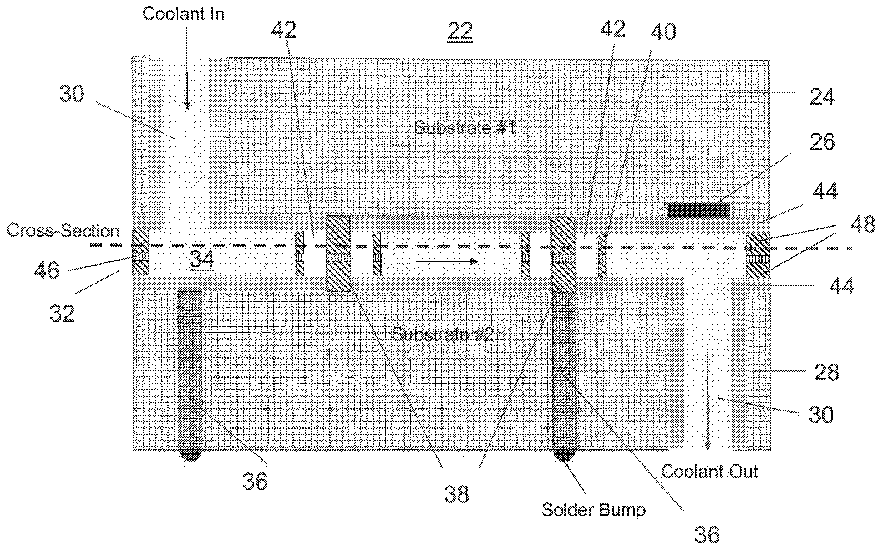
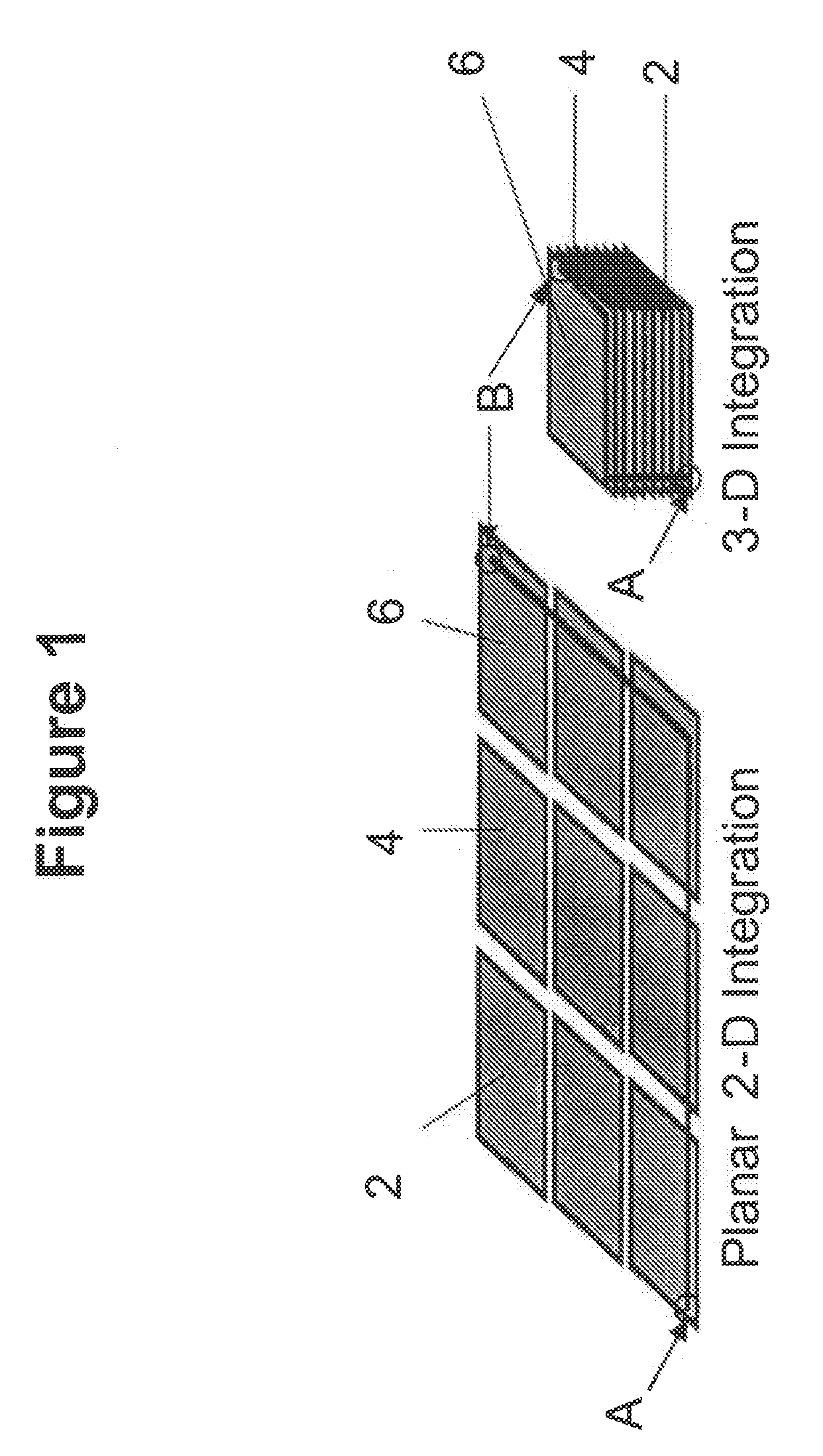
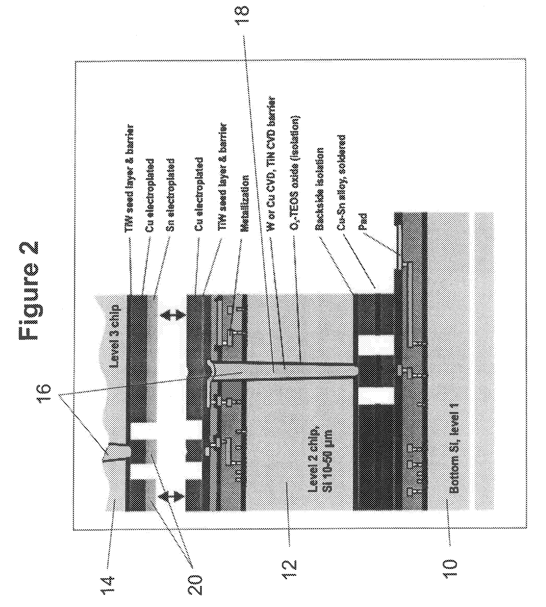
[0040]The problem of extracting heat from an integrated circuit (IC) can be a significant problem, especially as the circuit density (and the waste heat dissipation) for chip sets are increasing. This problem is expected to be significantly more severe in 3D integrated circuits where the volumetric density of active and passive devices is dramatically increased and / or the thermal path length from an active device to the surface can be considerably longer. The problem is apparent in IC production past the 65 nm node in addition to current high performance devices at older IC production nodes, higher power analog / mixed signal ICs, IR focal plane arrays, or any structure that has required liquid or air cooling directly behind a functional or non-functional substrate.

[0041]More specifically, 3D circuits pose thermal management challenges due to the increase in total power generated per available surface area for cooling. In addition, the power generated per unit volume within the 3D cir...


PUM


Abstract

A structure and method for thermal management of integrated circuits. The structure for thermal management of integrated circuits includes first and second substrates bonded together, at least one of the first and second substrates including at least one circuit element, an entrance through-hole having a length extending through a thickness of at least one of the first substrate and the second substrate, an exit through-hole having a length extending through a thickness of at least one of the first substrate and the second substrate, a bonding element forming a seal between the first and second substrates and forming a space between the first and second substrate, and a coolant channel formed in the space between the first and second substrates such that a fluid entering the entrance through-hole transits the coolant channel and the exit through-hole to provide cooling to the circuit element. The method supplies a fluid through the entrance through-hole, flows the fluid through the coolant channel between the first substrate and second substrates, and removes the fluid from the coolant channel through the exit through-hole.

Description

DISCUSSION OF THE BACKGROUND[0001]1. Field of the Invention[0002]This invention relates to devices and methods for the management of thermal loads in stacked integrated circuits.[0003]2. Background of the Invention[0004]Interconnect delays are increasingly dominating IC performance due to increases in chip size and reduction in minimum feature size. The interconnect structures on chips are consuming more and more of the available power and delay budgets. Further, the global and semi global wires generally dominate the delay and power budgets of circuits.[0005]An emerging architecture / technology attempting to alleviate these issues is three-dimensional (3D) integration. 3D integration represents a system level integration scheme in which multiple layers of integrated circuits (IC) are stacked and interconnected to each other in the stack or vertical direction. Thus, a large number of the long horizontal interconnects commonly used in two-dimensional (2D) structures are replaced by sh...

Claims


Application Information

Patent Timeline
Patent Type & Authority Applications(United States)
IPC IPC(8): H01L23/34H01L21/46H05K7/20
CPCH01L23/473H01L23/481H01L2924/13091H01L2224/0401H01L2224/131H01L25/0657H01L2225/06513H01L2225/06589H01L2924/09701H01L2224/05H01L2224/02372H01L2224/05548H01L2224/13H01L2224/13024H01L2224/13025H01L2224/14181H01L2224/16145H01L2224/16146H01L2924/014H01L2924/00
Inventor GARROU, PHILIPWILLIAMS, CHARLES KENNETHBOWER, CHRISTOPHER A.
Owner MICROSS ADVANCED INTERCONNECT TECH LLC
Why Eureka
Try Eureka