Circuit Combining Level Shift Function with Gated Reset

a technology of gated reset and circuit, applied in logic circuits, logic circuit coupling/interface arrangements, pulse techniques, etc., can solve problems such as power-needy devices such as pfet devices, exacerbate problems, and reduce the area of power-needy devices, so as to reduce the number of large pfet devices and reduce the number of complex functions. , the effect of reducing the number of devices

Inactive Publication Date: 2009-03-05
IBM CORP
View PDF3 Cites 2 Cited by
  • Summary
  • Abstract
  • Description
  • Claims
  • Application Information

AI Technical Summary

Benefits of technology

[0007]Thus a circuit according to the invention combining level shift function with gated reset performs a simple logic function such as ‘and’, ‘or’ with inputs supplied from a lower voltage VD and a drive out at its output with a higher voltage VC. Said circuit comprises a gated reset scheme that reduces the number of large p-doped devices such as PFETs for logic function to one.
[0008]Advantages of the circuit according to the invention over the state of the art are that the circuit allows more complex functions than a level shifter circuit, such as a simple logic function like ‘and’, ‘or’, possible with inputs supplied from a lower supply voltage VD. Further, the circuit according to the invention uses a gated reset scheme that reduces the number of large PFET devices for logic function to one. Compared with state of the art circuits, where in order to perform an ‘or’ function a stack of three p devices are required, two for the or function and one for the level shift function, with the circuit according to the invention a significant reduction in devices and thus area requirement is achieved. Additionally, the circuit according to the invention has no DC current in quiet state. Also compared to the state of the art, the circuit according to the invention has a higher circuit speed.

Problems solved by technology

This problem can be exacerbated with wider gates in which multiple PFETs could be on and leaking DC current.
Additionally level shifter circuits with more complex functions are desired, allowing a reduction of area and thus power needy devices such as PFET devices.

Method used


Image

  • Circuit Combining Level Shift Function with Gated Reset
  • Circuit Combining Level Shift Function with Gated Reset
  • Circuit Combining Level Shift Function with Gated Reset

Examples


Embodiment Construction

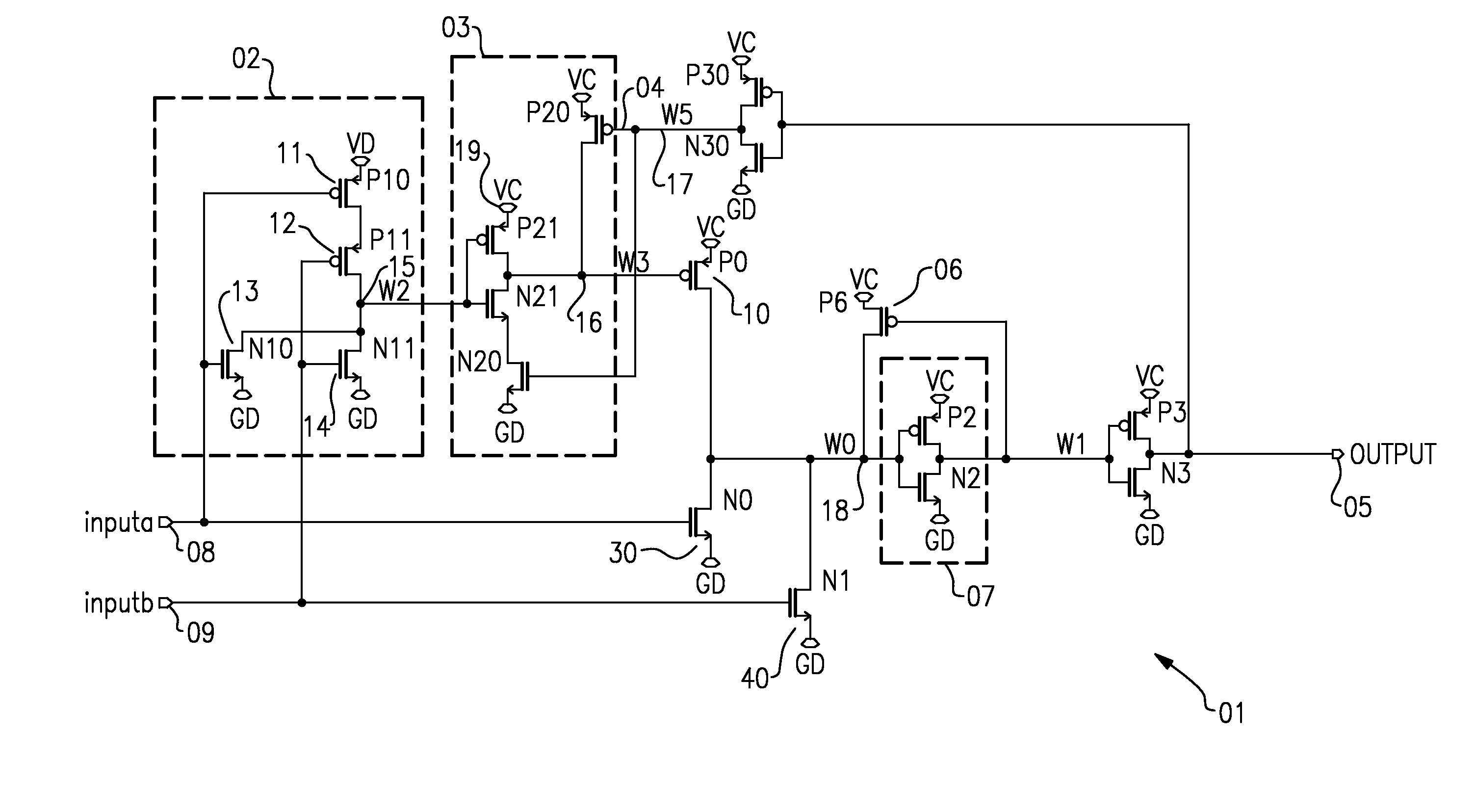
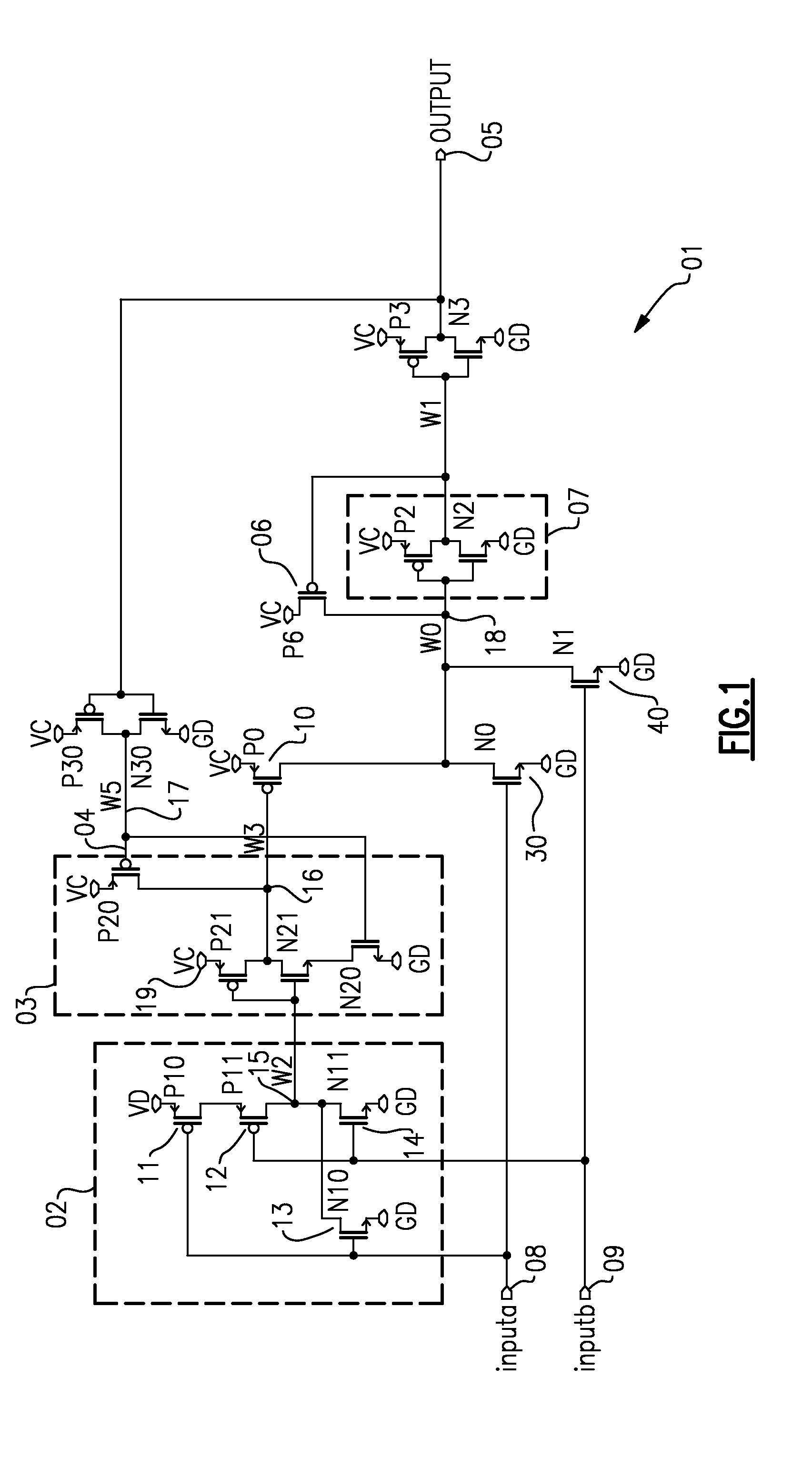
[0014]A circuit 01 combining level shift function with gated reset shown in FIG. 1 performs a simple logic function such as ‘and’, ‘or’ with inputs supplied from a lower voltage VD and drives an output 05 to or from a high voltage VC. The circuit 01 uses a gated reset scheme that reduces the number of large p-doped devices such as PFETs for logic function to one. The device within the circuit 01 for logic function is the PFET P010. Further devices for logic functions ‘and’, ‘or’ are the devices N030 and N140. The gated reset scheme is implemented by a reset gate 02, formed by the devices P1011, P1112, N1013, N1114 driving the node W215, duplicating the logic function but with small devices. It drives a NAND gate 03 whose other input 04 is the inverted feed back from the output 05. Thus the gated reset function is implemented. But the NAND gate 03 takes also care that node W316 is always on high voltage VC except during reset transition.

[0015]Reset, which for the circuit 01 is that t...


PUM


Abstract

A circuit (01) combining level shift function with gated reset is described, performing a simple logic function with inputs supplied from a lower voltage (VD) and a drive out at its output (05) with a higher voltage (VC). Said circuit (01) comprises a gated reset scheme plus devices (10, 30, 40) for logic function.

Description

BACKGROUND OF THE INVENTION[0001]The invention relates to a circuit combining level shift function with gated reset.[0002]Within microprocessors scaling of the power supply voltage occurs for power reduction and reliability reasons. Certain types of circuits are more sensitive to this reduction in voltage such as analog, memory and chip input / output (I / O) and / or receiving / driving circuits. To combat this, many chip designs have added extra power supply domains to use in these sensitive circuits.[0003]If static logic gates are connected normally at the interface between a lower supply voltage VD and a higher supply voltage VC, as VC rises greater than a PFET (P-doped Field Effect Transistor) threshold voltage above VD, the PFET will turn on and a direct current (DC) will flow through the gate connected to VC. This will prevent a good down level on the output node. This problem can be exacerbated with wider gates in which multiple PFETs could be on and leaking DC current. Because of t...

Claims


Application Information

Patent Timeline
Patent Type & Authority Applications(United States)
IPC IPC(8): H03K19/0185
CPCH03K19/018521H03K19/0013
Inventor FROEHNEL, THOMASMAYER, GUENTERSAUTTER, ROLFWAGNER, OTTO
Owner IBM CORP
Why Eureka
Try Eureka