Plasma Display Device

a display device and plasma technology, applied in the direction of instruments, static indicating devices, etc., can solve problems such as complicated circuit configuration, and achieve the effect of simple circuit configuration and high impedance states

Inactive Publication Date: 2009-03-05
HITACHI LTD
View PDF8 Cites 4 Cited by
  • Summary
  • Abstract
  • Description
  • Claims
  • Application Information

AI Technical Summary

Benefits of technology

[0014]According to the present invention, by the first switch circuit and the second switch circuit, it is possible to control the scan electrode of the even display line and the scan electrode of the odd display line independently to make the scan electrodes be in high impedance states. Thereby, a discharge of the even display line is restrained in a sustain period of an odd frame and a discharge of the odd display line is restrained in a sustain period of an even frame, so that an interlace drive can be realized with a simple circuit configuration.

Problems solved by technology

As shown in FIG. 16, it is necessary to provide two sustain circuits in the Y electrode driver and the X electrode driver respectively, leading to a complicated circuit configuration.

Method used


Image

  • Plasma Display Device
  • Plasma Display Device
  • Plasma Display Device

Examples


first embodiment

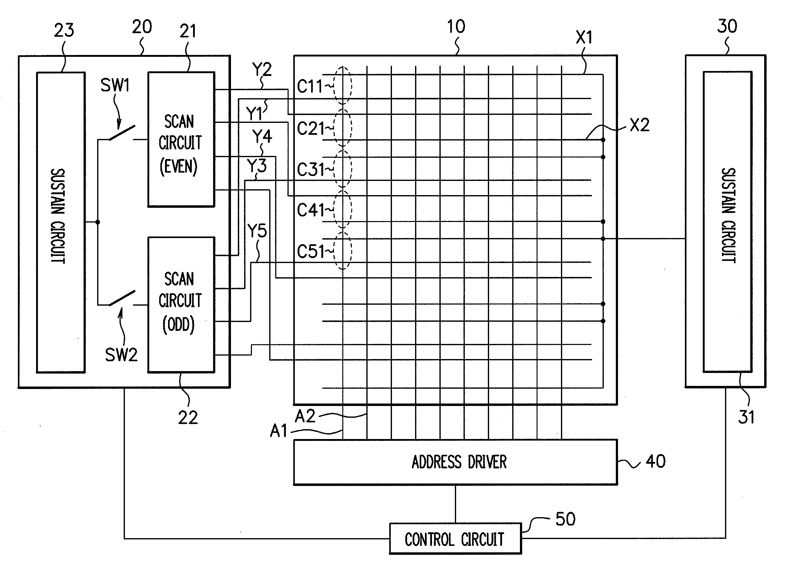
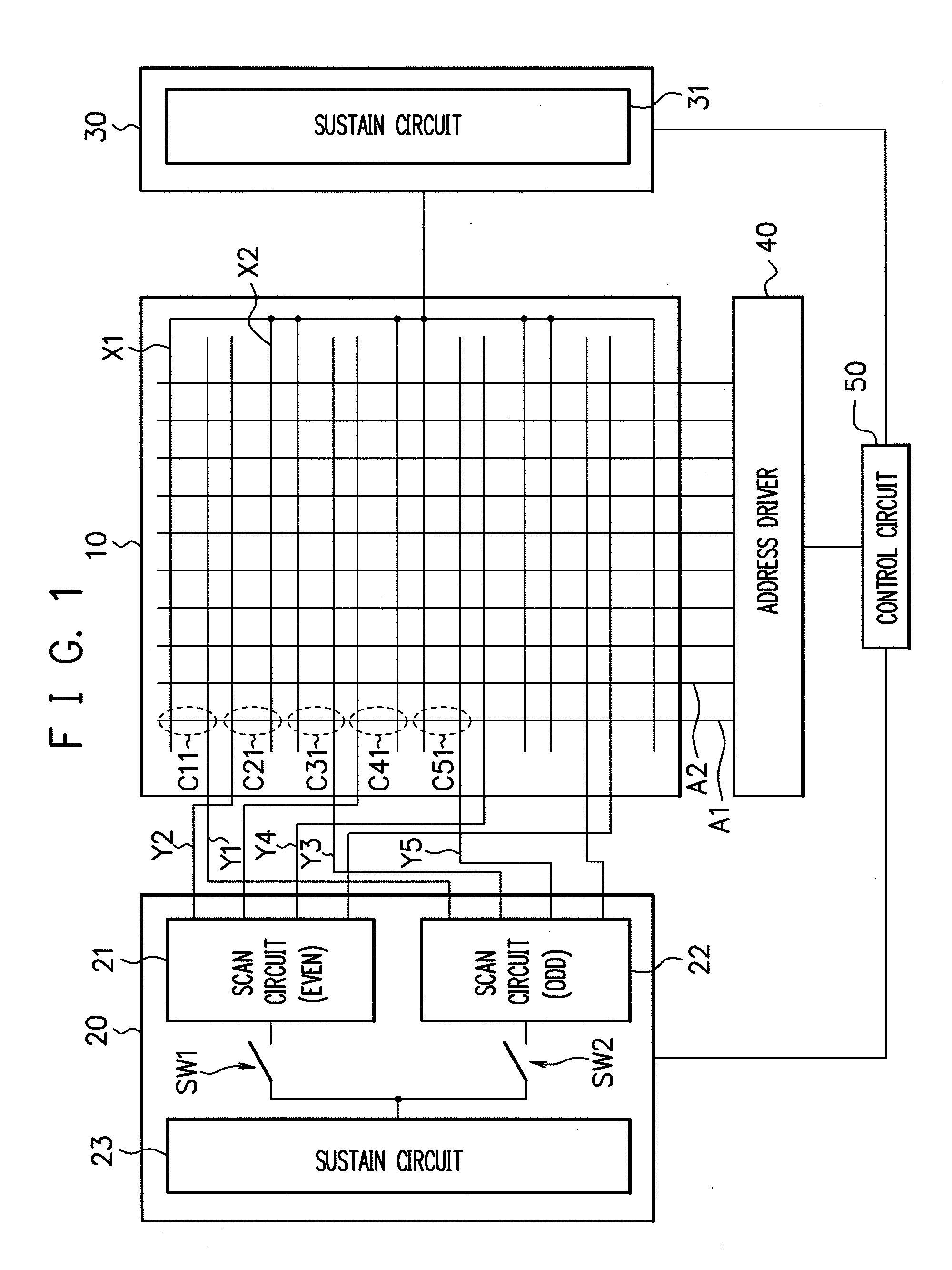
[0034]FIG. 1 is a block diagram showing a configuration example of a plasma display device according to a first embodiment of the present invention. The plasma display device according to the first embodiment has a plasma display panel 10, a Y electrode driver 20, an X electrode driver 30, an address driver 40 and a control circuit 50.

[0035]The Y electrode driver 20 is a circuit to drive Y electrodes (scan electrodes) Y1, Y2, . . . among display electrodes. The Y electrode driver 20 has a scan circuit (even) 21, a scan circuit (odd) 22 and a sustain circuit 23. Hereinafter, each of the Y electrodes Y1, Y2, . . . is also referred to or generically named as a Y electrode Yi, the i meaning a subscript.

[0036]The scan circuits 21, 22 are constituted with circuits performing line-sequential scanning to select a row to be displayed. The sustain circuit 23 is constituted with a circuit repeating sustain discharges. Predetermined voltages are supplied to a plurality of Y electrodes Yi by the...

second embodiment

[0071]Next, a second embodiment of the present invention will be described.

[0072]In the above-described first embodiment, in the sustain period of the odd frame the switch SW1 is made to be in the OFF state to make the Y electrode Yi (Ye) of the even display line be in the high impedance state, while in the sustain period of the even frame the switch SW2 is made to be in the OFF state to make the Y electrode Yi (Yo) of the odd display line be in the high impedance state.

[0073]In contrast, in the second embodiment described below, a sustain period is divided into a first sustain period and a second sustain period. It is controlled that in the first sustain period sustain pulses are applied to both of Y electrodes Yi (Ye, Yo) of even display line and odd display line, and in the second sustain period the Y electrode Yi (Ye) of the even display line is made to be high impedance in a case of an odd frame while the Y electrode Yi (Yo) of the odd display line is made to be high impedance ...

third embodiment

[0087]Next, a third embodiment of the present invention will be described.

[0088]In the third embodiment, similarly to in the second embodiment, a sustain period is divided into a first sustain period and a second sustain period. In the first sustain period, it is controlled that sustain pulses are applied to both of Y electrodes Yi (Ye, Yo) of an even display line and an odd display line. In the second sustain period, it is controlled that a sustain pulse is applied to the Y electrode Yi (Yo) of the odd display line to make the Y electrode Yi (Ye) of an even display line be in a high impedance state in a case of an odd frame, and that a sustain pulse is applied to the Y electrode Yi (Ye) of the even display line to make the Y electrode Yi (Yo) of the odd display line be in the high impedance state in a case of an even frame.

[0089]In other words, in the first sustain period of the odd frame, in a Y electrode driver 20, both a switch SW1 to connect a scan circuit (even) 21 and a susta...


PUM


Abstract

Between a sustain circuit outputting a sustain pulse and a scan circuit (even) driving a Y electrode of an even display line, there is provided a first switch capable of making the Y electrode of the even display line be in a high impedance state, and between the sustain circuit and a scan circuit (odd) driving a Y electrode of an odd display line, there is provided a second switch capable of making the Y electrode of the odd display line be in the high impedance state. By first and second switches, the Y electrode of the even display line and the Y electrode of the odd display line can be independently controlled to be in the high impedance states, whereby discharge of the even display line can be restrained in a sustain period of an odd frame, while a discharge of the odd display line can be restrained in a sustain period of an even frame, thereby realizing an interlace drive without complicating a circuit configuration.

Description

CROSS-REFERENCE TO RELATED APPLICATIONS[0001]This application is based upon and claims the benefit of priority from the prior Japanese Patent Application Nos. 2007-221656, filed on Aug. 28, 2007, and 2007-299707, filed on Nov. 19, 2007, the entire contents of which are incorporated herein by reference.BACKGROUND OF THE INVENTION[0002]The present invention relates to a plasma display device.[0003]Among plasma display panels (PDPs), there is a common electrode type plasma display panel (hereinafter, also referred to as “common electrode panel”), which has an electrode structure where neighboring cells have a common electrode (for example, see Japanese Patent Application Laid-open No. Hei 9-160525).[0004]FIG. 16 is a block diagram showing a configuration of a plasma display device having a common electrode panel. The plasma display device has a plasma display panel (common electrode panel) 110, a Y electrode driver 120, an X electrode driver 130, an address driver 140, and a control ci...

Claims


Application Information

Patent Timeline
Patent Type & Authority Applications(United States)
IPC IPC(8): G09G3/28G09G3/288G09G3/296G09G3/298G09G3/299
CPCG09G3/296G09G3/2983G09G2330/022G09G2310/0224G09G3/299
Inventor HASHIMOTO, YASUNOBUKIMURA, MASAKIKISHI, TOMOKATSUITO, KATSUMIITOKAWA, NAOKIOHKI, HIDEAKI
Owner HITACHI LTD
Why Eureka
Try Eureka