Method and apparatus for circuit simulation in view of stress exerted on MOS transistor

a mos transistor and circuit simulation technology, applied in the field of circuit simulation based on the stress exerted on the mos transistor, can solve the problems of reducing the accuracy of circuit simulation and not achieving highly accurate circuit simulation, and achieve the effect of high-accuracy circuit simulation

Inactive Publication Date: 2009-04-02
RENESAS ELECTRONICS CORP
View PDF6 Cites 14 Cited by
  • Summary
  • Abstract
  • Description
  • Claims
  • Application Information

AI Technical Summary

Benefits of technology

[0015]The present invention realizes highly accurate circuit simulation, appropriat

Problems solved by technology

In recent years, increasing attention has been paid to effects of the stress exerted on an MOS transistor, which is one of the causes which reduce circuit simulation accuracy.
According to the study of the

Method used


Image

  • Method and apparatus for circuit simulation in view of stress exerted on MOS transistor
  • Method and apparatus for circuit simulation in view of stress exerted on MOS transistor
  • Method and apparatus for circuit simulation in view of stress exerted on MOS transistor

Examples


Embodiment Construction

[0029]The invention will be now described herein with reference to illustrative embodiments. Those skilled in the art will recognize that many alternative embodiments can be accomplished using the teachings of the present invention and that the invention is not limited to the embodiments illustrated for explanatory purposes.

1. Outline of Circuit Simulation

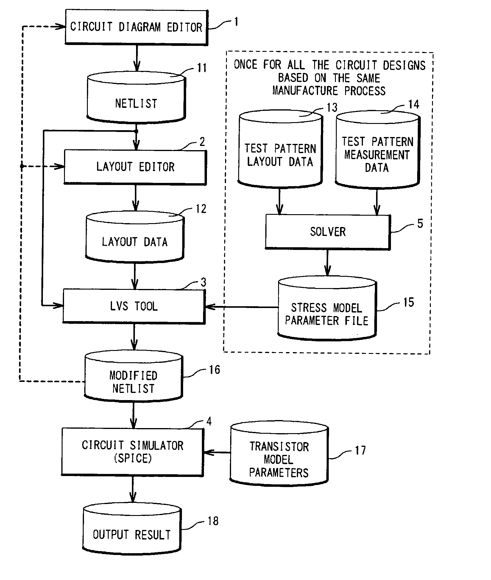
[0030]Referring to FIG. 1, a description is first given of an outline of circuit simulation in one embodiment of the present invention.

[0031]FIG. 1 shows an exemplary layout of an MOS transistor. In FIG. 1, the reference numeral 30 denotes an MOS transistor to be subjected to circuit simulation. The reference numeral 31 denotes an active region of the MOS transistor 30 and the reference numeral 32 denotes the gate of the MOS transistor 30. The gate 32 is provided so as to cross the active region 31. The active region 31 includes a portion which functions as a channel region of the MOS transistor 30, disposed just beneath the gate 3...


PUM


Abstract

A circuit simulation method includes: generating graphical data indicating dimensions of a subject MOS transistor; calculating a parameter correction amount based on said graphical data; correcting a given transistor model parameter in response to said parameter correction amount; and performing circuit simulation of a circuit that includes said subject MOS transistor by using said corrected transistor model parameter. The parameter correction amount is calculated based on said graphical data by using arithmetic equations. The arithmetic equations include at least one stress model equation expressing a stress exerted on a channel region of a model MOS transistor. The stress model equation is suitably defined to simulate the stress exerted on the channel region.

Description

INCORPORATION BY REFERENCE[0001]This application claims the benefit of priority based on Japanese Patent Application No. 2007-258117, filed on Oct. 1, 2007, the disclosure of which is incorporated herein by reference.BACKGROUND OF THE INVENTION[0002]1. Field of the Invention[0003]The present invention relates to a method and apparatus for circuit simulation, more particularly, to circuit simulation based on stress exerted on MOS transistors.[0004]2. Description of the Related Art[0005]Circuit simulation is one of the important techniques in the development of semiconductor integrated circuits. An operation of a designed semiconductor integrated circuit is checked by circuit simulation to confirm whether the subject semiconductor integrated circuit satisfies design specifications. This allows developing semiconductor integrated circuits with desired functions and performances.[0006]A typical procedure of circuit simulation is as follows: First, characteristics of respective MOS trans...

Claims


Application Information

Patent Timeline
IPC IPC(8): G06F17/50
CPCG06F17/5036G06F30/367
Inventor YAMADA, KENTA
Owner RENESAS ELECTRONICS CORP
Why Eureka
Try Eureka