Method for designing semiconductor integrated circuit and method of circuit simulation

a technology of integrated circuits and circuits, applied in the field of semiconductor integrated circuits, can solve problems such as large property discrepancies, and achieve the effects of high accuracy, simplified model parameter extraction means, and high simulation accuracy

Inactive Publication Date: 2008-01-24
PANASONIC CORP
View PDF3 Cites 61 Cited by
  • Summary
  • Abstract
  • Description
  • Claims
  • Application Information

AI Technical Summary

Benefits of technology

[0016]This method uses, when executing a parameter extraction from the gate protrusion portion by using a parameter of applied stress to a channel, a simple model expression showing an inverse proportion between the change rate of a saturated current value and a sum of the gate protrusion length and a product of the gate width of the actually measured transistor and a coefficient A. This enables a highly accurate simulation that into consideration effects to an operation of a transistor by stress applied to the channel from the gate protrusion portion can be performed.
[0017]Thus, the operation of an integrated circuit can be simulated with high accuracy by modeling change of a transistor property depending on a gate protrusion length with use of a simple model expression. Also for a complicated gate wiring patterns existing in actual LSIs, the model parameter extraction means is simplified and the amount of calculation is reduced by using such a procedure that assumes, for a gate electrode with a gate contact pad and a gate electrode with a bent wiring, that the gate protrusion length is infinite. This facilitates a highly accurate circuit simulation.

Problems solved by technology

However, ongoing refinement has posed a new problem; there is caused a great discrepancy of properties between an ideal independent transistor for extracting model parameters and a CMOS type transistor included in a cell of practical design.

Method used


Image

  • Method for designing semiconductor integrated circuit and method of circuit simulation
  • Method for designing semiconductor integrated circuit and method of circuit simulation
  • Method for designing semiconductor integrated circuit and method of circuit simulation

Examples


first embodiment

—Method for Designing—

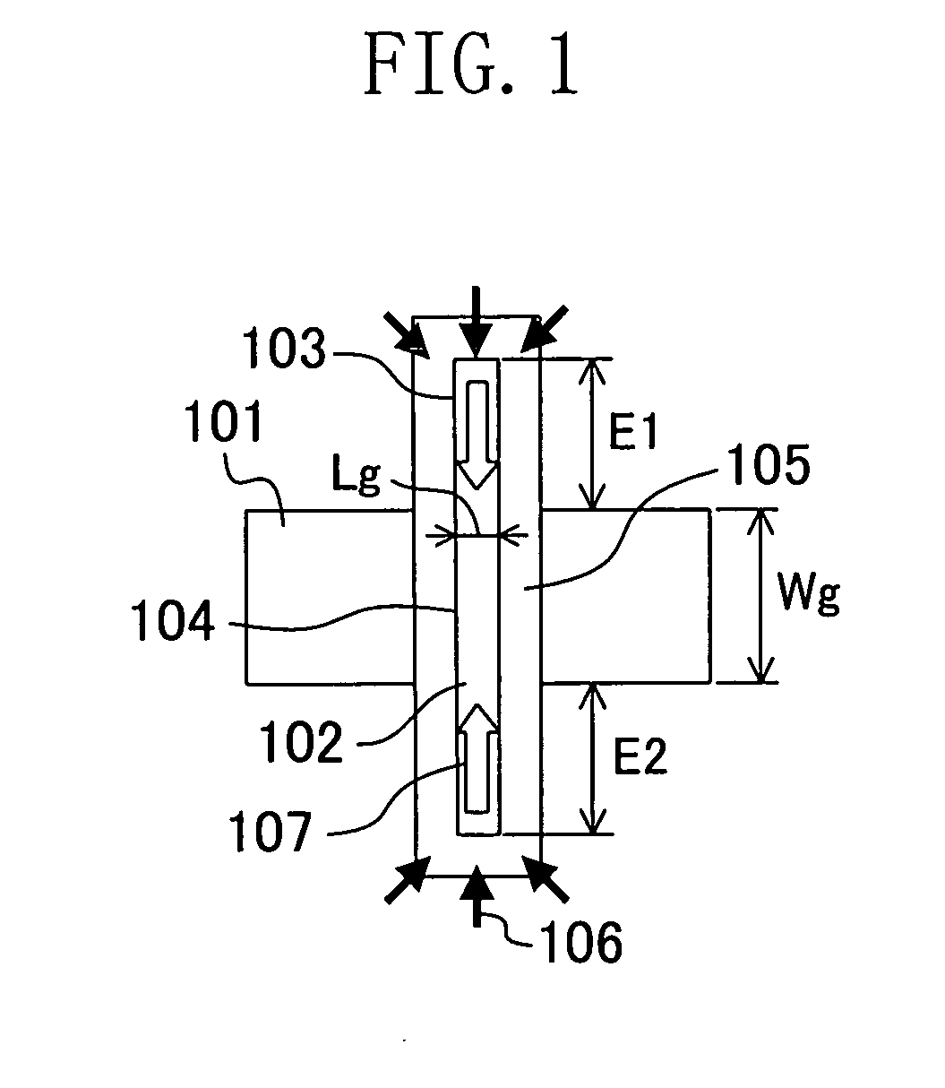
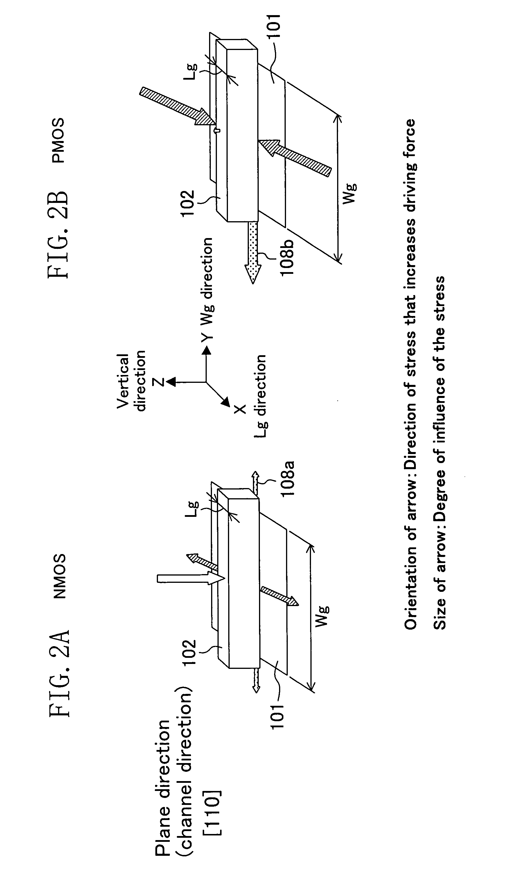
[0032]FIG. 1 is a plan view explaining how stress is applied to an end of a gate. The figure shows a MOS transistor (hereinafter simply referred to as a transistor 104) including an active region 101 formed on a semiconductor substrate, a gate electrode 102 formed on the semiconductor substrate by interleaving a gate insulation film, and a side wall 105 formed on a side of the gate electrode 102. The side wall 105 is made of, for example, SiN. In FIG. 1, reference numeral 103 denotes a gate protrusion portion, reference numeral 106 denotes compressive stress arising in the side wall 105 when the side wall 105 contracts, and reference numeral 107 denotes compressive stress applied to the gate protrusion portion 103 from the side wall 105. In addition, Lg denotes a gate length, Wg denotes a gate width, E1 and E2 denote gate protrusion lengths in both side of a transistor in a direction of the gate width.

[0033]In a method for designing a semiconductor integrated c...

second embodiment

—Procedure of a Method for Designing—

[0054]As a second embodiment of the present invention, a modeling method for a complicated gate wiring pattern used in an actual LSI will be explained. Two patterns of a gate contact pad shape and a bent wiring shape are considered as a complicated gate wiring pattern. By considering the two patterns, all gate wiring patterns can be dealt with.

[0055]FIGS. 6A to 6C are views showing examples of patterns of transistors having a gate electrode 102 with a gate contact pad 109. In the figures, a length of one end of the gate electrode 102 with the gate contact pad 109 is a gate protrusion length E2, and a length of another end of the gate electrode 102 is a gate protrusion length E1. In addition, FIG. 7A shows a pattern of a transistor 104 whose one end has a gate contact pad 109 and whose another end has a L type bent wiring 113, and FIG. 7B shows a pattern of a transistor 104 whose one end has a gate contact pad 109 and whose another end has a T typ...

third embodiment

[0078]As a third embodiment of the present invention, a method for executing a circuit simulation with use of the method for designing explained in the first and second embodiments.

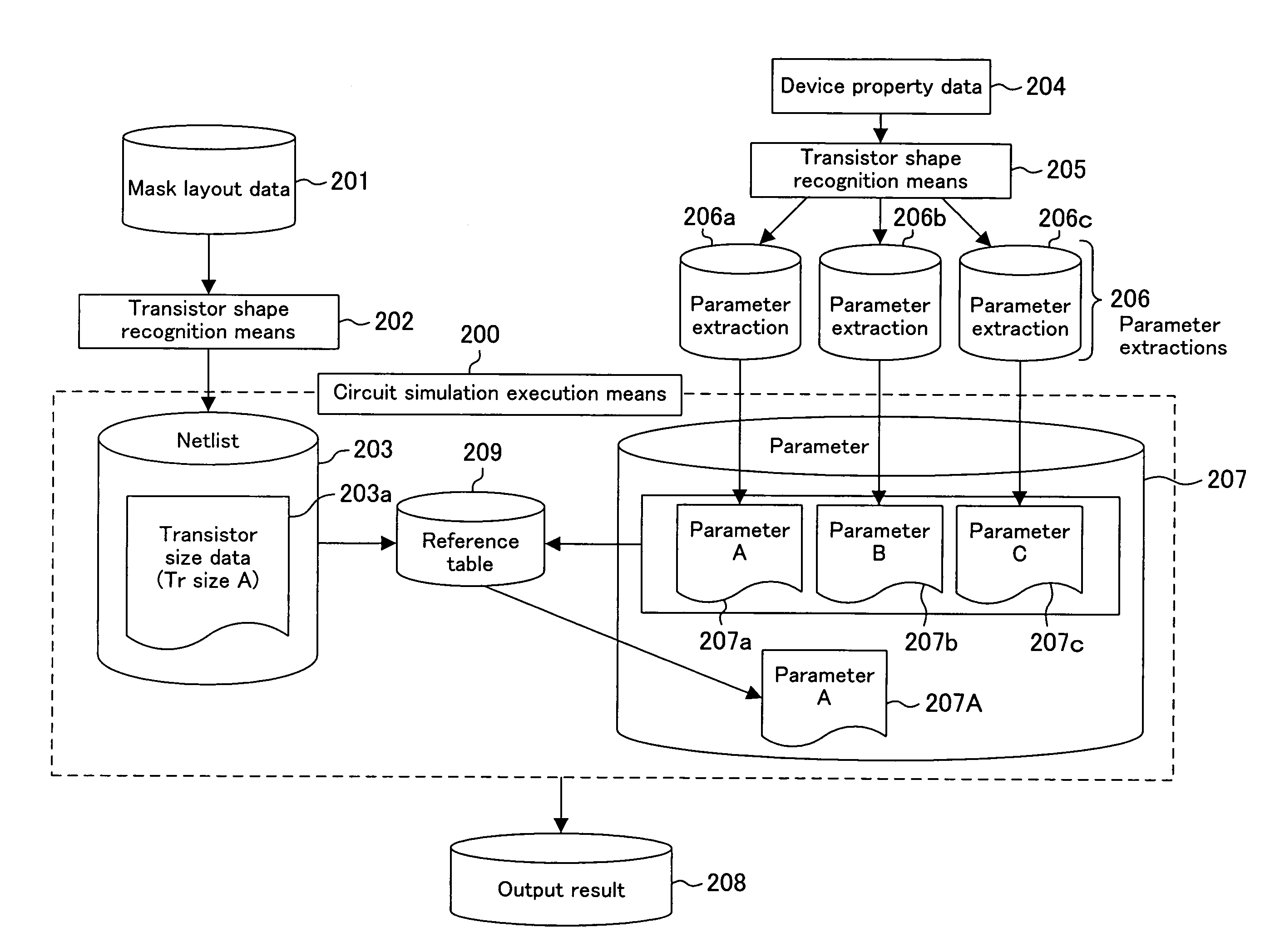
[0079]FIG. 12 is a block diagram showing a configuration of a circuit simulation device according to a third embodiment. As shown in the figure, the circuit simulation device includes a circuit simulation execution means 200.

[0080]A netlist extracted from a mask layout data 201 by designing tools or the like and a parameter 207 extracted from device property data 204 that is an actual measured value of a device property are inputted to the circuit simulation execution means 200.

[0081]Specifically, transistor size data 203a is extracted by a first transistor shape recognition means 202 from the mask layout data 201 having designing data of a circuit to be analyzed, and the transistor size data 203a is inputted to the circuit simulation execution means 200 as represented by the SPICE or the like as a netlis...


PUM


Abstract

By using, as a model expression, an expression showing an inverse proportion between a change rate ΔIdsat/Idsat of saturated current value and a product of a gate protrusion length E1 and a gate width Wg of a transistor and a coefficient, modeling is executed for a transistor property that depends on the gate protrusion length. This provides a circuit simulation that takes into consideration the gate protrusion length of a gate electrode.

Description

BACKGROUND OF THE INVENTION[0001]1. Technical Field[0002]The present invention relates to a method for designing a semiconductor integrated circuit in which a multiplicity of MIS transistors are integrated.[0003]2. Related Art[0004]An LSI (Large Scale Integrated) represented by a microprocessor is a combination of a multiplicity of unit circuits generally referred to as cells, which have basic functions. In accordance with high integration and high performance for the LSI, CAD (Computer Aided Design) tools play increasingly important rolls for highly accurate circuit design of a cell, which is an essential part of circuit design of the LSI.[0005]A circuit simulator is used as one of the CAD tools associated in high degree with design accuracy. The circuit simulator simulates operations of a designed cell and LSI on the basis of a netlist including connection information of elements such as MOS (Metal Oxide Semiconductor) transistor, capacitative elements, and resistance elements, an...

Claims


Application Information

Patent Timeline
Patent Type & Authority Applications(United States)
IPC IPC(8): G06F17/50
CPCG06F17/5063G06F17/5036G06F30/36G06F30/367
Inventor YAMASHITA, KYOJIIKOMA, DAISAKUSAHARA, YASUYUKIOOTANI, KATSUHIROWATANABE, SHINJI
Owner PANASONIC CORP
Why Eureka
Try Eureka