Channel stress engineering using localized ion implantation induced gate electrode volumetric change

a technology of volumetric change and channel stress, applied in the direction of basic electric elements, electrical equipment, semiconductor devices, etc., can solve the problems of reducing the dimensions of field effect devices, reducing the accuracy of mechanical stress effects, and difficult to reliably and uniformly reproduce mechanical stress effects

Inactive Publication Date: 2009-04-09
GLOBALFOUNDRIES INC
View PDF5 Cites 14 Cited by
  • Summary
  • Abstract
  • Description
  • Claims
  • Application Information

AI Technical Summary

Benefits of technology

[0010]The invention provides a semiconductor structure and method for fabricating the semiconductor structure. The method for fabricating the semiconductor structure includes use of an ion implantation method for implanting a volumetric change ion into a portion of a gate electrode that is located over a channel region within a semiconductor substrate to provide a volumetrically changed ion implanted material portion of the gate electrode that has a first stress that induces a second stress different than the first stress within the channel region within the semiconductor substrate. Particular variations of an embodiment of the invention use particular volumetric change ion implanting species to form the volumetrically changed ion implanted material portion of the gate electrode that

Problems solved by technology

In that regard, mechanical stress effects are often difficult to reliably and uniformly reproduce as fi

Method used


Image

  • Channel stress engineering using localized ion implantation induced gate electrode volumetric change
  • Channel stress engineering using localized ion implantation induced gate electrode volumetric change
  • Channel stress engineering using localized ion implantation induced gate electrode volumetric change

Examples


Embodiment Construction

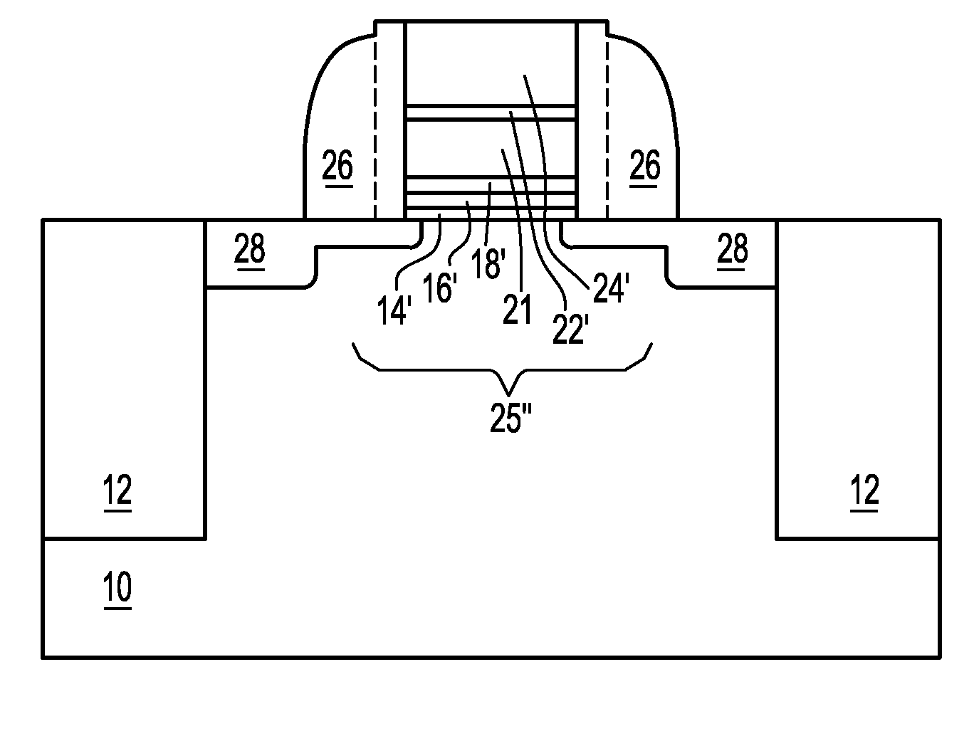
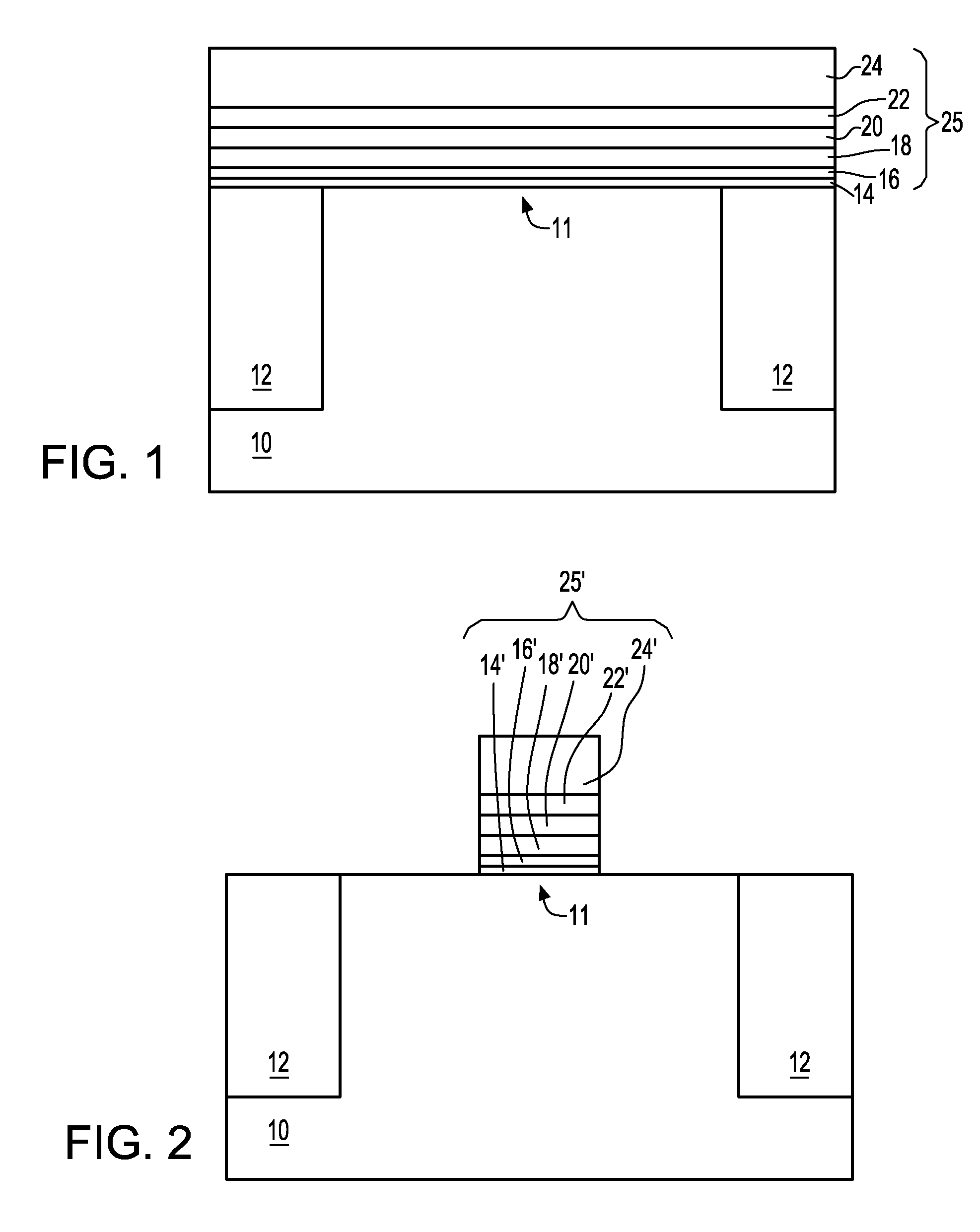
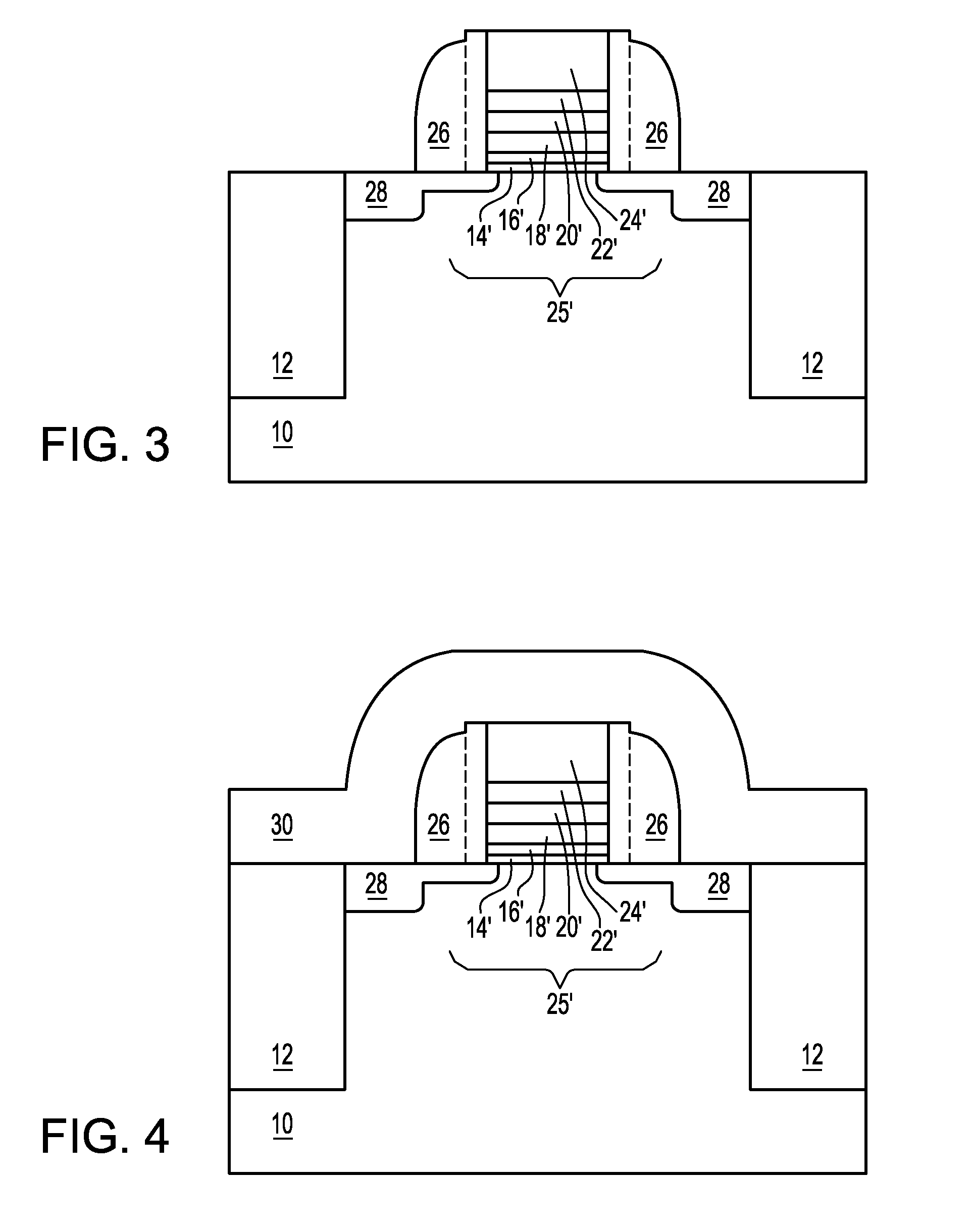
[0017]The invention, which includes: (1) a semiconductor structure that includes a gate electrode a portion of which has a first stress that induces a second stress different than the first stress within a channel region of a semiconductor substrate over which is located the gate electrode; and (2) a method for fabricating the semiconductor structure that includes the above described gate electrode, is understood within the context of the description set forth below. The description set forth below is understood within the context of the drawings described above. Since the drawings are intended for illustrative purposes, the drawings are not necessarily drawn to scale.

[0018]FIG. 1 to FIG. 9 show a series of schematic cross-sectional diagrams illustrating the results of progressive stages in fabricating a semiconductor structure in accordance with a particular embodiment of the invention. This particular embodiment of the invention comprises a sole embodiment of the invention.

[0019]F...


PUM


Abstract

A method for fabricating a semiconductor structure uses a volumetric change ion implanted into a volumetric change portion of a gate electrode that is located over a channel region within a semiconductor substrate to form a volume changed portion of the gate electrode located over the channel region within the semiconductor substrate. The volume changed portion of the gate electrode is typically bidirectionally symmetrically graded in a vertical direction. The volume-changed portion of the gate electrode has a first stress that induces a second stress different than the first stress into the channel region of the semiconductor substrate.

Description

BACKGROUND[0001]1. Field of the Invention[0002]The invention relates generally to channel stress within field effect devices. More particularly, the invention relates to efficient methods for inducing channel stress within field effect devices.[0003]2. Description of the Related Art[0004]Field effect devices, such as but not limited to field effect transistor devices, are common semiconductor devices that are used within semiconductor circuits. In particular, field effect transistor devices have been effectively scaled in dimension over the period of several decades to provide semiconductor circuits with increasing levels of integration and increasing levels of functionality.[0005]Recent advances in performance of field effect devices have focused upon both a selection of a particular crystallographic orientation of a semiconductor substrate upon which is fabricated a field effect device, as well as introduction of a particular channel stress within the particular crystallographic o...

Claims


Application Information

Patent Timeline
IPC IPC(8): H01L29/78H01L21/3205
CPCH01L21/265H01L21/28061H01L29/7845H01L29/517H01L29/7833H01L29/4941
Inventor LUO, ZHIJIONGZHU, HUILONG
Owner GLOBALFOUNDRIES INC
Why Eureka
Try Eureka