Optical device and manufacturing method thereof

a manufacturing method and optical technology, applied in the field of optical devices, can solve the problems of increased manufacturing cost, high glass plate cost, and inability of optical devices to receive or emit blue-violet laser light, and achieve the effect of convenient and reliable manufacturing

Active Publication Date: 2009-04-16
PANNOVA SEMIC
View PDF16 Cites 20 Cited by
  • Summary
  • Abstract
  • Description
  • Claims
  • Application Information

AI Technical Summary

Benefits of technology

[0016]According to the invention, a method for manufacturing an optical device including an optical element having an optical function region on one surface, and a wiring board having the optical element mounted thereon and electrically connected to the optical element includes the steps of: mounting another surface of the optical element on the wiring board; electrically connecting the optical element with the wiring board; and resin-sealing at least an electrically connected portion of the optical element and the wiring board by using a mold. The mold includes a lower mold that is placed on an opposite surface of an optical element mounting surface of the wiring board, and an upper mold for placing the wiring board having the optical element mounted thereon between the upper mold and the lower mold. In the resin-sealing step, a sheet is interposed between the upper mold and the wiring board. The upper mold has a projection that presses the sheet against the optical function region. With this structure, an optical device having an exposed optical function region as a bottom surface can be easily and reliably manufactured.

Problems solved by technology

However, such optical devices cannot be used to receive or emit blue-violet laser light having a wavelength as short as 405 nanometers (nm) because transparent resin discolors with time and the transmittance changes.
However, such a glass plate is very expensive, and the manufacturing cost is increased.
In manufacturing of the optical function element module described in Japanese Laid-Open Patent Publication No. 2006-186288, it is difficult to control dropping of the liquid sealing resin so as to form a desired amount of sealing resin with a desired shape only within a desired range.
This results in reduction in yield.
However, this makes it impossible to achieve size reduction which is one of the objects of Japanese Laid-Open Publication No. 2006-186288.

Method used


Image

  • Optical device and manufacturing method thereof
  • Optical device and manufacturing method thereof
  • Optical device and manufacturing method thereof

Examples


first embodiment

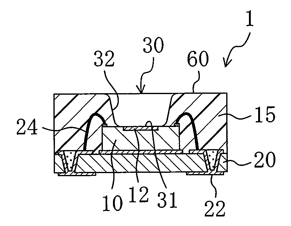
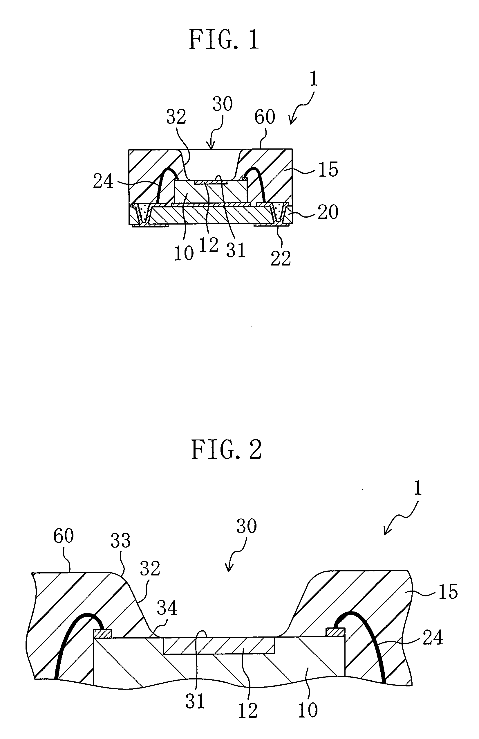
[0029][Structure of an Optical Device]

[0030]FIG. 1 is a cross-sectional view of an optical device 1 according to a first embodiment of the invention. FIG. 2 is an enlarged cross-sectional view showing an upper part of the optical device 1. The optical device 1 is formed by resin-sealing an optical element (light-receiving element) 10 mounted on a wiring board 20 with a sealing resin 15 so as to expose an optical function region (light-receiving portion) 12.

[0031]The optical element 10 that is a semiconductor element has a rectangular flat plate shape. The optical function region 12 is formed in the center of one surface of the optical element 10. Electrode pads are provided on the periphery of this surface of the optical element 10. The optical element 10 is fixed to the wiring board 20 by mounting the other surface of the optical element 10 (the surface on which the optical function region 12 is not formed) on the wiring board 20. In other words, the optical element 10 is mounted o...

second embodiment

[0051]An optical device 2 of a second embodiment shown in FIGS. 6A and 6B is substantially the same as the optical device 1 of the first embodiment except the shape of an optical function region 14 of an optical element 11. Therefore, only the differences from the first embodiment will be described below and description of the same portions will be omitted.

[0052]In the optical device 2 of this embodiment, the optical function region 14 is formed at the bottom of a recessed portion 43 formed in the center of a light-receiving surface of the optical element 11. A region surrounding the recessed portion 43 on the light-receiving surface is a recessed-portion peripheral surface portion 71. As shown in FIG. 6B, when resin sealing is performed, the sheet 90 abuts on the whole optical function region 14 and a recessed-portion sidewall 42 due to the flexibility of the sheet 90. The sheet 90 (and the protrusion 55 behind the sheet 90) rises upward from the recessed-portion sidewall 42. There...

third embodiment

[0055]An optical device 3 of a third embodiment shown in FIGS. 7A and 7B is substantially the same as the optical device 1 of the first embodiment except the shape of an optical function region 16 of an optical element 13. Therefore, only the differences from the first embodiment will be described below and description of the same portions will be omitted.

[0056]In the optical device 3 of this embodiment, the optical function region 16 is formed at the top surface of a protruding portion 48 provided in the center of a light-receiving surface of the optical element 13. A region surrounding the protruding portion 48 on the light-receiving surface is a protruding-portion peripheral surface portion 72. As shown in FIG. 7B, when resin sealing is performed, the sheet 90 abuts on the whole optical function region 16 and on a sidewall 47 of the protruding portion 48 due to the flexibility of the sheet 90. Therefore, a boundary portion 34 between a side surface 32 of a recess 45 and a bottom ...


PUM

PropertyMeasurementUnit
thicknessaaaaaaaaaa
optical functionaaaaaaaaaa
areaaaaaaaaaaa

Abstract

An optical element mounted on a wiring board is sealed by a sealing resin except an optical function region. Wires connecting the wiring board with the optical element are also sealed by the sealing resin. The optical function region is exposed as a bottom surface of a recess whose side surface is formed by the sealing resin. A boundary portion between the side surface of the recess and a top surface portion and a boundary portion between the side surface and bottom surface of the recess have a rounded shape.

Description

BACKGROUND OF THE INVENTION[0001]1. Field of the Invention[0002]The invention relates to an optical device and a manufacturing method thereof. More particularly, the invention relates to an optical device including an optical element and a wiring board having the optical element mounted thereon, in which an electrically connected portion of the optical element and the wiring board is resin-sealed, and a manufacturing method of the optical device.[0003]2. Related Art[0004]Optical devices having an optical semiconductor device, such as a solid state imaging element and an LED (Light Emitting Diode), mounted on a wiring board have been known in the art. An example of such an optical device has a hollow package structure in which a light-transmitting substrate is provided over an optical function surface in order to protect the optical function surface (for example, see Japanese Laid-Open Patent Publication Nos. 2003-332542 and 2006-303481). In another example of such an optical device,...

Claims


Application Information

Patent Timeline
Patent Type & Authority Applications(United States)
IPC IPC(8): G02B7/00B29D11/00H01L33/54H01L33/56H01L33/62
CPCB29C45/14418H01L2224/48227B29C2045/14663H01L24/97H01L27/14618H01L27/14683H01L31/0203H01L31/18H01L33/52H01L33/54H01L2224/48091H01L2224/92247H01L2224/97H01L2924/01013H01L2924/01018H01L2924/01029H01L2924/01033H01L2924/01078H01L2924/01082H01L2924/1815B29C45/14655H01L2924/12041H01L2924/01006H01L2924/01005H01L2924/00014H01L2224/85H01L2224/83
Inventor MINAMIO, MASANORIISHIDA, HIROYUKIYOSHIKAWA, NORIYUKI
Owner PANNOVA SEMIC
Why Eureka
Try Eureka