Process for manufacturing a wiring substrate

a manufacturing process and wiring substrate technology, applied in the direction of printed circuit manufacturing, insulating substrate metal adhesion improvement, conductive pattern formation, etc., can solve the problem of difficult roughening treatment for making the wiring pattern layer into a finer pitch, and achieve the effect of keeping the shaping precision and the sizing precision of the wiring pattern layer reliably

Inactive Publication Date: 2005-05-19
NGK SPARK PLUG CO LTD
View PDF3 Cites 6 Cited by
  • Summary
  • Abstract
  • Description
  • Claims
  • Application Information

AI Technical Summary

Benefits of technology

[0012] According to this process, the vicinities of the intercrystalline boundaries, in which impurities in the copper plating agglomerate, are etched deeper than 1 μm in a crack shape, but a thickness of 1 μm or less is removed at the surfaces of the crystal grains surrounded by the vicinities. Thus, it is possible to keep the shaping precision and the sizing precision of the wiring pattern layers reliably.
[0013] According to the invention, there is further provided, as a preferable embodiment, a wiring substrate manufacturing process, wherein a narrow one of the plated resists has a width of less than 20 μm, and wherein one narrow wiring line in the wiring pattern layers etched has a width of less than 20 μm. According to this process, it is possible to reliably provide a wiring substrate having wiring pattern layers of a fine pitch.

Problems solved by technology

As a result, this adhesion could be retained, but that roughening treatment was difficult for making the wiring pattern layer into a finer pitch.

Method used


Image

  • Process for manufacturing a wiring substrate
  • Process for manufacturing a wiring substrate
  • Process for manufacturing a wiring substrate

Examples


Embodiment Construction

[0031] The best mode for carrying out the invention will be described in the following.

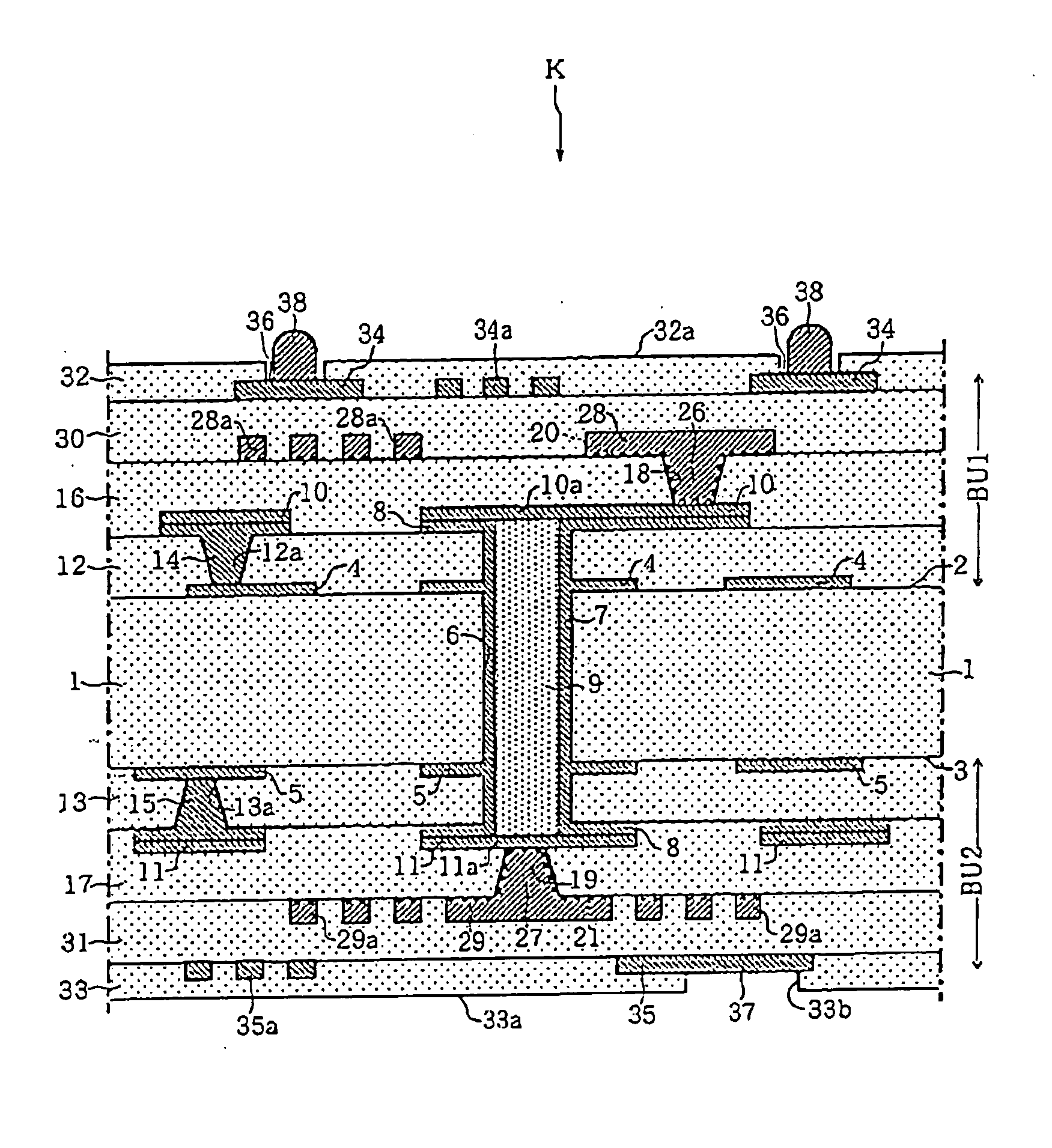
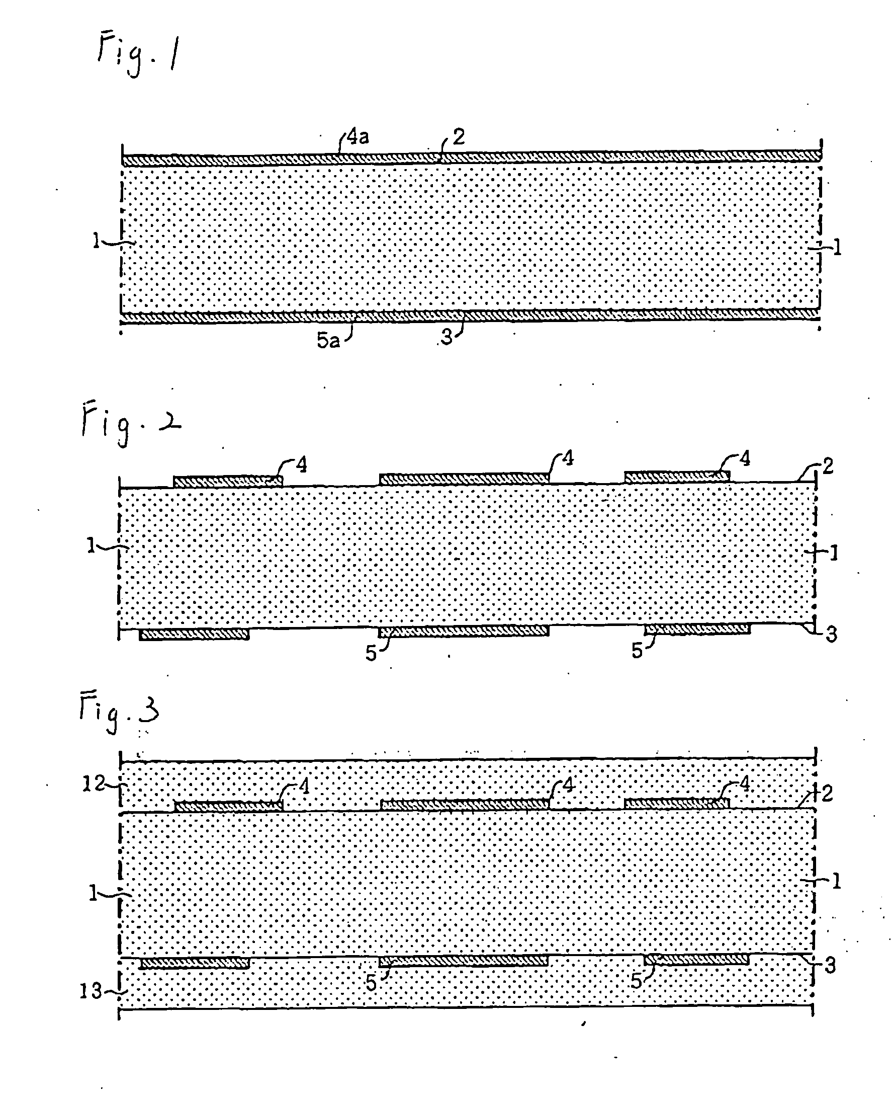
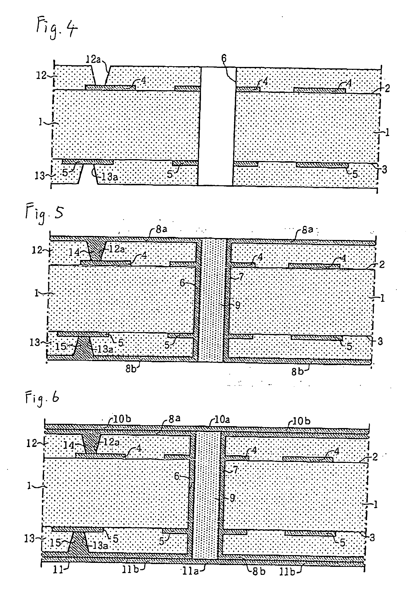
[0032]FIG. 1 is a section showing a core substrate 1 made of a bismaleimide triazine (BT) resin having a thickness of about 0.7 mm. This core substrate 1 is covered on its surface 2 and a back 3, respectively, with copper foils 4a and 5a having a thickness of about 70 μm. The not-shown photosensitive / insulating dry film is formed over those copper foils 4a and 5a and is subjected to an exposure and a development of a predetermined pattern. After this, the etching resist obtained is removed with a peeling liquid (according to the well-known subtractive method).

[0033] Here, a multi-panel having a plurality of core substrates 1 may be used so that the individual core substrates 1 may be subjected to a similar treatment step (as in the following individual steps).

[0034] As a result, the copper foils 4a and 5a become wiring layers 4 and 5 profiling the aforementioned pattern, as shown in FIG. 2.

[00...


PUM

PropertyMeasurementUnit
thicknessaaaaaaaaaa
widthaaaaaaaaaa
length×a widthaaaaaaaaaa

Abstract

A process for manufacturing a wiring substrate, comprising: a step of forming thin copper film layers on surfaces of insulating resin layers by plating the same electrolessly with copper; a step of forming plated resists of a pattern over the thin copper film layers; a step of forming wiring pattern layers in clearances of the plated resists by plating the same electrolytically with copper; a step of removing the plated resists and the thin copper film layers just below the plated resists; a step of etching surfaces of the wiring pattern layers to remove a thickness of 1 μm or less from the wiring pattern layers; and a step of forming another insulating resin layers over the insulating resin layers and the wiring pattern layers etched.

Description

FIELD OF THE INVENTION [0001] The present invention relates to a wiring substrate manufacturing process capable of forming a wiring pattern layer (or a built-up wiring layer) easily at a fine pitch. BACKGROUND ART BACKGROUND OF THE INVENTION [0002] According to the trend of recent years for a high performance and a high signal-processing rate, there has been enhanced a demand for making the size of the wiring substrate smaller and the pitch of the wiring pattern layers finer. [0003] For example, an insulating resin layer between one wiring pattern layer and an adjacent wiring pattern layer is generally restricted by a practical limit of the section of a length×a width of 25 μm×25 μm. However, it has been demanded that the length and the width are individually 20 μm or less. [0004] In order to satisfy these demands, it is necessary not only to form the wiring pattern layer precisely in shape and size but also to make the etching allowance small and homogenous for roughening the surfa...

Claims


Application Information

Patent Timeline
Patent Type & Authority Applications(United States)
IPC IPC(8): H05K3/18C23F1/18C25D5/02H05K3/10H05K3/38H05K3/46
CPCC23F1/18C25D5/022H05K3/108Y10T29/49156H05K3/4602H05K2203/0353Y10T29/49155H05K3/383
Inventor SAIKI, HAJIMESUGIMOTO, ATSUHIKO
Owner NGK SPARK PLUG CO LTD
Why Eureka
Try Eureka