Method for manufacturing a resistor random access memory with a self-aligned air gap insulator

Active Publication Date: 2009-04-23
MACRONIX INT CO LTD
View PDF16 Cites 134 Cited by
  • Summary
  • Abstract
  • Description
  • Claims
  • Application Information

AI Technical Summary

Benefits of technology

[0019]In embodiments of memory cells described herein including phase change material memory elements, the active region of the memory element can be made extremely small, thereby reducing the amount of current needed for reset. The extremely small active region is a result of the memory element having a width preferably less than a minim

Problems solved by technology

Problems have arisen in manufacturing devices with very small dimensions, and with vari

Method used


Image

  • Method for manufacturing a resistor random access memory with a self-aligned air gap insulator
  • Method for manufacturing a resistor random access memory with a self-aligned air gap insulator
  • Method for manufacturing a resistor random access memory with a self-aligned air gap insulator

Examples


Embodiment Construction

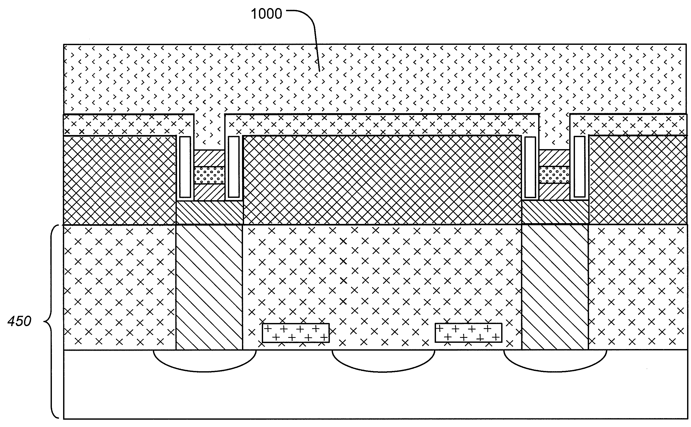
[0027]A description of structural embodiments and methods of the present invention is provided with reference to FIGS. 1-12. It is to be understood that there is no intention to limit the invention to the specifically disclosed embodiments but that the invention may be practiced using other features, elements, methods and embodiments. Like elements in various embodiments are commonly referred to with like reference numerals.

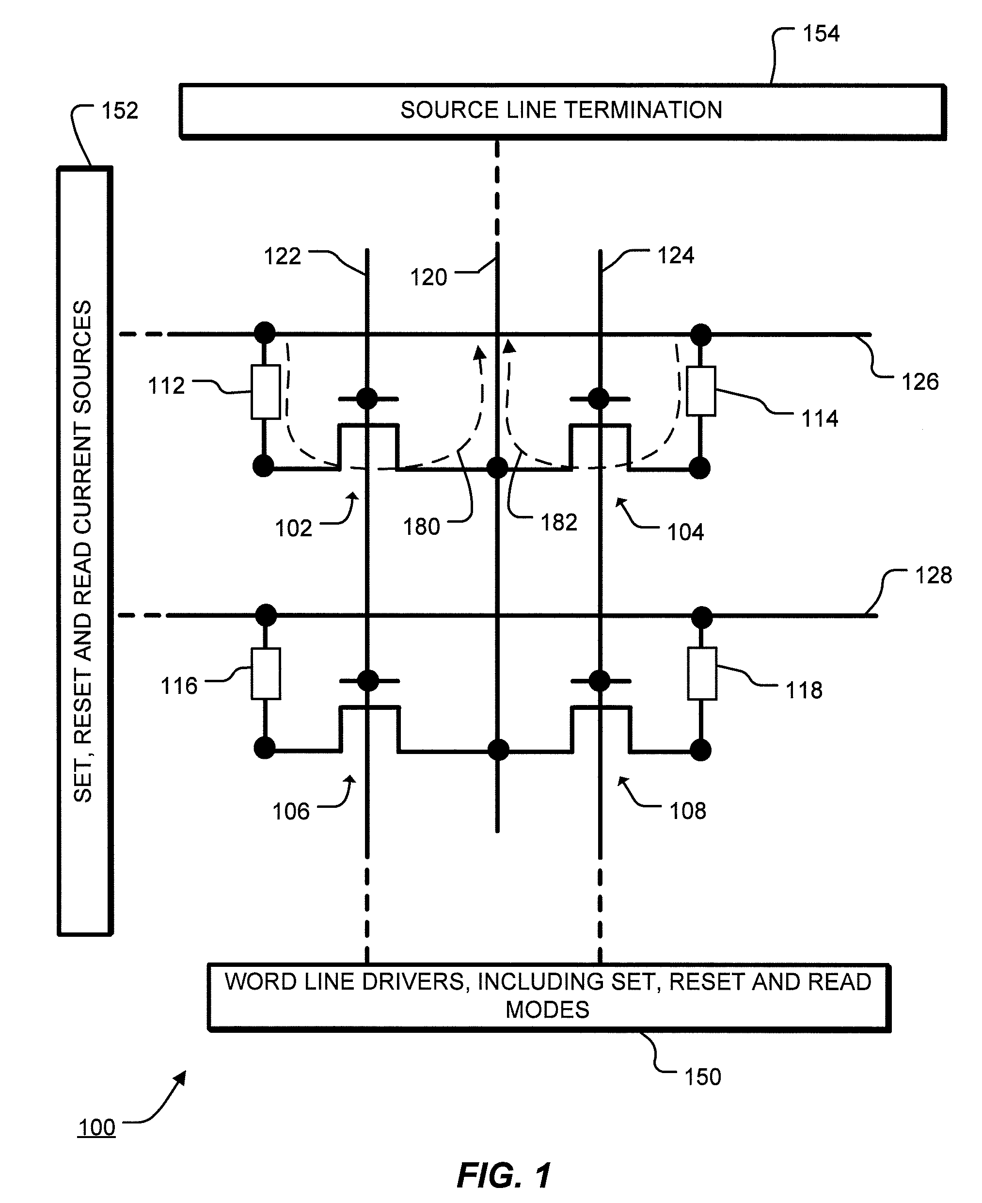
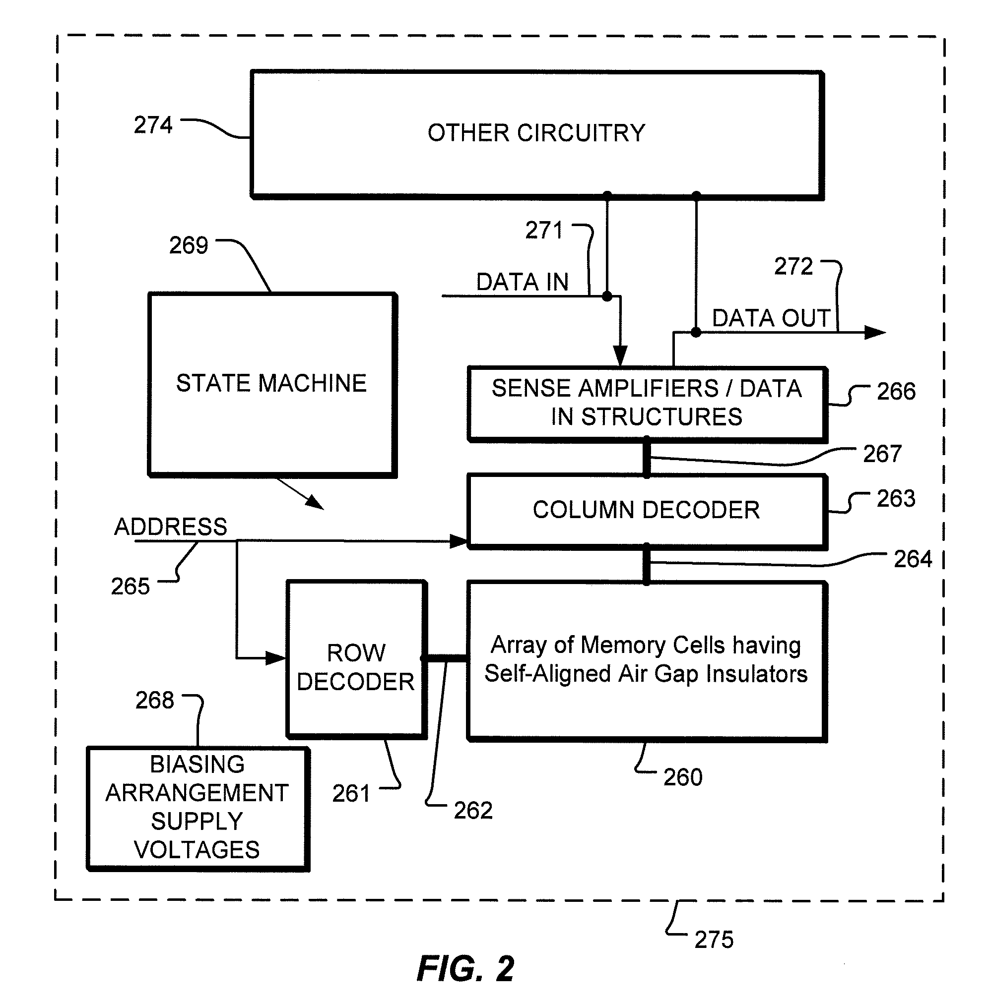
[0028]FIG. 1 is a schematic illustration of a memory array 100, which can be implemented using memory cells having self aligned air gaps as described herein. Four memory cells 102, 104, 106, and 108 having respective memory elements 112, 114, 116, and 118 each having respective self aligned air gaps (not shown) are illustrated in FIG. 1, representing a small section of an array that can include millions of memory cells.

[0029]In the schematic illustration of FIG. 1, common source line 120 and word lines 122, 124 are arranged generally parallel in the y-direction. ...


PUM


Abstract

A memory device including a programmable resistive memory material is described along with methods for manufacturing the memory device. A memory device disclosed herein includes top and bottom electrodes and a multilayer stack disposed between the top and bottom electrodes. The multilayer stack includes a memory element comprising programmable resistive memory material and has a sidewall surface. An air gap is adjacent to the sidewall surface and self-aligned to the memory element.

Description

REFERENCE TO RELATED APPLICATION[0001]This application claims the benefit of U.S. patent application Ser. No. 11 / 552,356 filed 24 Oct. 2006, entitled METHOD FOR MANUFACTURING A RESISTOR RANDOM ACCESS MEMORY WITH A SELF-ALIGNED AIR GAP, by inventors Erh-Kun Lai, Chiahua Ho, and Kuang-yeu Hsieh, for which a Request for Conversion to provisional status was filed on 1 Mar. 2007.BACKGROUND OF THE INVENTION[0002]1. Field of the Invention[0003]The present invention relates generally to electrically programmable and erasable memory, and more particularly, to memory having a small programmable resistive memory material with a self-aligned air gap.[0004]2. Description of Related Art[0005]Phase change based memory materials are widely used in read-write optical disks. These materials have at least two solid phases, including for example a generally amorphous solid phase and a generally crystalline solid phase. Laser pulses are used in read-write optical disks to switch between phases and to re...

Claims


Application Information

Patent Timeline
IPC IPC(8): H01L21/28H01L45/00
CPCH01L45/06H01L45/1233H01L45/126H01L45/1675H01L45/144H01L45/148H01L45/1293H10N70/231H10N70/8413H10N70/8616H10N70/826H10N70/884H10N70/8828H10N70/063
Inventor LAI, ERH KUNHO, CHIAHUAHSIEH, KUANG YEU
Owner MACRONIX INT CO LTD
Why Eureka
Try Eureka