Semiconductor light-emitting device and method of fabricating the same

a technology semiconductor light-emitting device, which is applied in the direction of semiconductor/solid-state device manufacturing, semiconductor devices, electrical equipment, etc., can solve the problems of high manufacturing cost of led b>1/b>, achieve enhanced light-emitting efficiency of semiconductor light-emitting device, increase light-emitting area, and improve current diffusion inside the semiconductor light-emitting devi

Inactive Publication Date: 2009-04-23
EPISTAR CORP
View PDF3 Cites 23 Cited by
  • Summary
  • Abstract
  • Description
  • Claims
  • Application Information

AI Technical Summary

Benefits of technology

[0013]Compared to the prior art, the semiconductor light-emitting device according to the invention has a largely increased light-emitting area, and the current diffusion inside the semiconductor light-emitting device is better. Thereby, the light-emitting efficiency of the semiconductor light-emitting device is enhanced. Moreover, the semiconductor light-emitting device according to the invention has the merits of an easier manufacturing process and lower cost.

Problems solved by technology

Furthermore, the etching process leads to a high manufacturing cost of the LED 1.

Method used


Image

  • Semiconductor light-emitting device and method of fabricating the same
  • Semiconductor light-emitting device and method of fabricating the same
  • Semiconductor light-emitting device and method of fabricating the same

Examples


Embodiment Construction

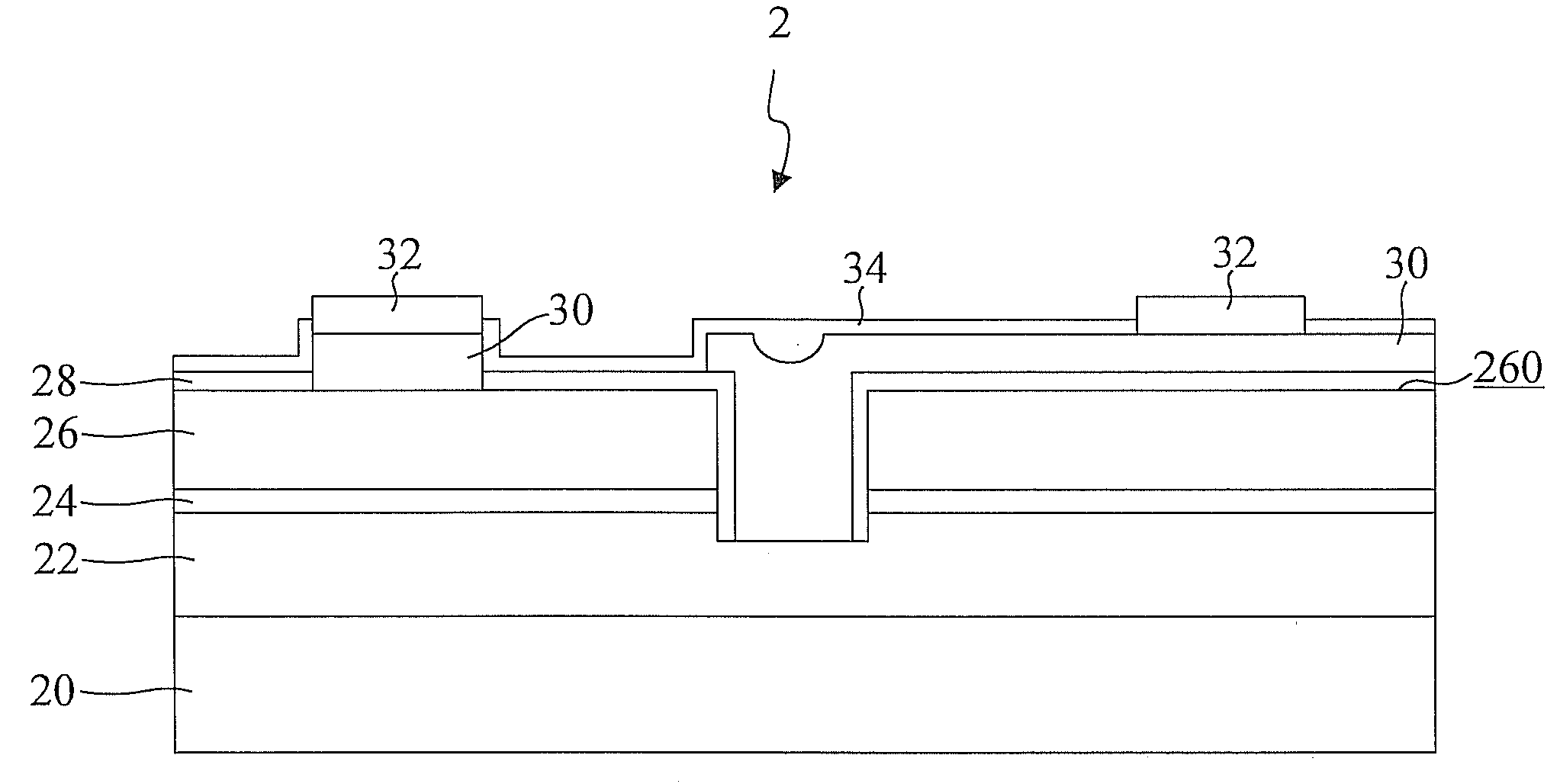
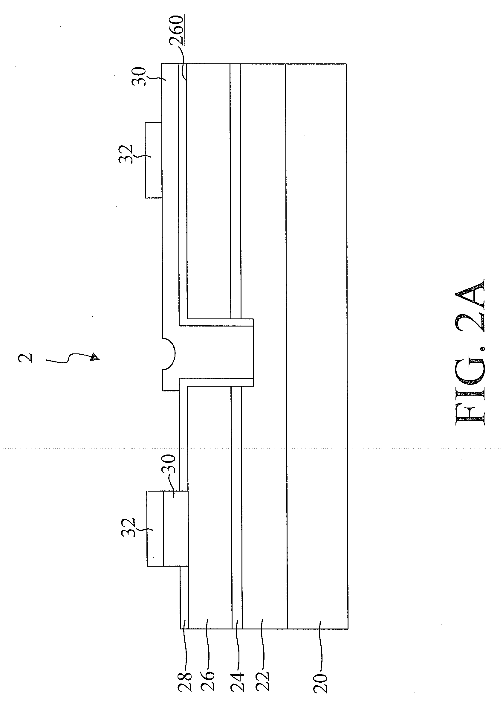
[0020]Please refer to FIG. 2A. FIG. 2A is a sectional view illustrating a semiconductor light-emitting device 2 according to an embodiment of the invention. In the embodiment, an LED is employed for the exemplification of the semiconductor light-emitting device 2, but not limited therein.

[0021]As shown in FIG. 2A, the semiconductor light-emitting device 2 includes a substrate 20, a first semiconductor material layer 22, a light-emitting layer 24, a second semiconductor material layer 26, a first transparent insulating layer 28, a metal layer 30 and at least one electrode 32.

[0022]In practical applications, the substrate 20 can be SiO2, Si, Ge, GaN, GaAs, GaP, AlN, sapphire, spinnel, Al2O3, SiC, ZnO, MgO, LiAlO2, LiGaO2, or MgAl2O4.

[0023]The first semiconductor material layer 22 is formed on the substrate 20. The light-emitting layer 24 is formed on the first semiconductor material layer 22. In one embodiment, the light-emitting layer 24 can be a PN-junction, a double hetero-junction...


PUM


Abstract

The invention discloses a semiconductor light-emitting device. The semiconductor light-emitting device includes a substrate, a first semiconductor material layer, a light-emitting layer, a second semiconductor material layer, a first transparent insulating layer, a metal layer and at least one electrode. The first semiconductor material layer, the light-emitting layer, and the second semiconductor material layer are formed in sequence on the substrate. An opening is formed on the upper surface of the second semiconductor material layer and extends to the interior of the first semiconductor material layer. The first transparent insulating layer overlays the sidewalls of the opening and substantially overlays the upper surface of the second semiconductor material layer such that a region of the upper surface is exposed. The metal layer fills the opening, overlays the exposed region, and partially overlays the first transparent insulating layer. The at least one electrode is formed on the metal layer.

Description

BACKGROUND OF THE INVENTION[0001]1. Field of the Invention[0002]The present invention relates to a semiconductor light-emitting device and, more particularly, to a semiconductor light-emitting device with a larger light-emitting area.[0003]2. Description of the Prior Art[0004]Nowadays, semiconductor light-emitting devices, such as Light Emitting Diodes (LEDs), have been used in a wide variety of applications, e.g., key systems, back light modules of mobile phone monitors, illuminating systems of vehicles, decorative lamps, and remote controls.[0005]Please refer to FIG. 1. FIG. 1 is a schematic diagram illustrating an LED 1 in the prior art. As shown in FIG. 1, the LED 1 includes a substrate 10, an N-type GaN layer 12, a P-type GaN layer 16, a light-emitting layer 14, and two electrodes 18. For the operation of the LED 1, the N-type GaN layer 12 and the P-type GaN layer 16 must be electrically conducted with each other in which a first electrode 18 is formed on the P-type GaN layer 1...

Claims


Application Information

Patent Timeline
Patent Type & Authority Applications(United States)
IPC IPC(8): H01L33/00H01L21/02H01L33/20H01L33/38H01L33/44
CPCH01L33/20H01L33/44H01L33/382
Inventor CHANG, HSUAN-TANG
Owner EPISTAR CORP
Why Eureka
Try Eureka