Test structures for e-beam testing of systematic and random defects in integrated circuits

a technology of integrated circuits and test structures, applied in the direction of individual semiconductor device testing, semiconductor/solid-state device testing/measurement, instruments, etc., can solve the problems of reducing the detection sensitivity of e-beam inspection, difficult to assess the impact of design of experiments on further dislocation density reduction,

Inactive Publication Date: 2009-04-23
TEXAS INSTR INC
View PDF1 Cites 111 Cited by
  • Summary
  • Abstract
  • Description
  • Claims
  • Application Information

AI Technical Summary

Benefits of technology

[0006]According to another embodiment of the present teachings, there is a semiconductor test structure for detecting current leakage paths. The semiconductor test structure can include one or more design elements accentuating localized, non-uniform stress in a semiconductor device, selected from the group consisting of active layer jogs, double active jogs with asymmetry, multiple active jogs, gate electrode turns over field dielectric regions, and H gate electrode turns over field dielectric regions. The semiconductor test structure can also include a substrate ground in close proximity to an active region including one or more of remote substrate grounds and substrate ground regions proximate to the active region.
[0007]According to yet another embodiment of the present teachings, there is a semiconductor test structure for detecting a contact-to-gate short including a p-type substrate, a plurality of floating gate electrodes, a plurality of grounded contacts through a dielectric layer, wherein a contact to gate electrode line spacing is less than or equal to a design rule, and a plurality of metal pads over the dielectric layer.
[0008]According to another embodiment of the present teachings, there is a semiconductor test structure for detecting a worm-hole. The semiconductor test structure can include a p-type substrate including a plurality of n-type active regions; a plurality of gate electrodes, wherein a gate electrode to gate electrode spacing is less than or equal to a design rule; a plurality of contacts through a dielectric layer; and a plurality of alternating grounded / floating rows of metal pads over the dielectric layer.
[0009]According to yet another embodiment of the present teachings, there is a semiconductor test structure for detecting troublesome pitches for hole printing during semiconductor processing. The semiconductor test structure can include a p-type substrate, a dielectric layer over the substrate, an array of grounded holes through the dielectric layer having a desired troublesome pitch, wherein the troublesome pitch is determined by one or more of an exposure conditions modeling and an empirical data, and a plurality of metal pads over the dielectric layer.

Problems solved by technology

However, the detection sensitivity of e-beam inspection is compromised by the lack of a substrate ground in close proximity to SRAM elements.
In addition, as process improvements are made, the SRAM cells become less sensitive indicators of the tendency to form dislocations so that it is difficult to assess the impact of design of experiments (DOEs) for further dislocation density reduction.

Method used


Image

  • Test structures for e-beam testing of systematic and random defects in integrated circuits
  • Test structures for e-beam testing of systematic and random defects in integrated circuits
  • Test structures for e-beam testing of systematic and random defects in integrated circuits

Examples


Embodiment Construction

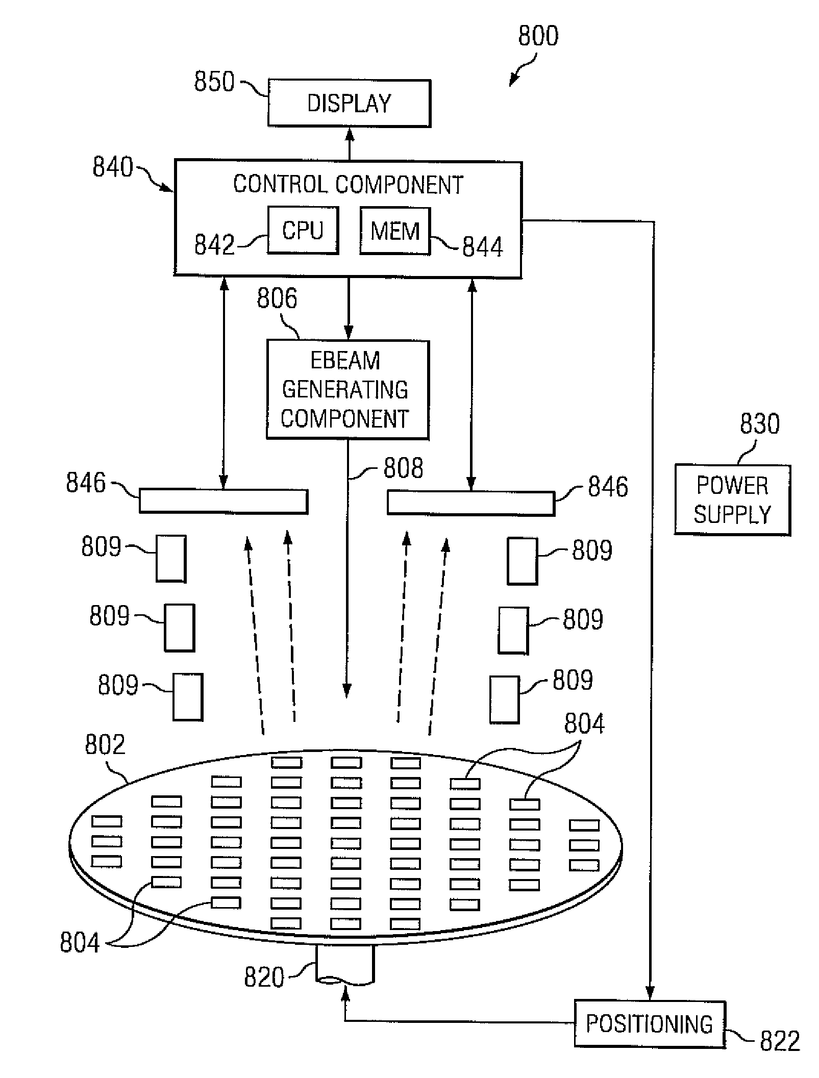
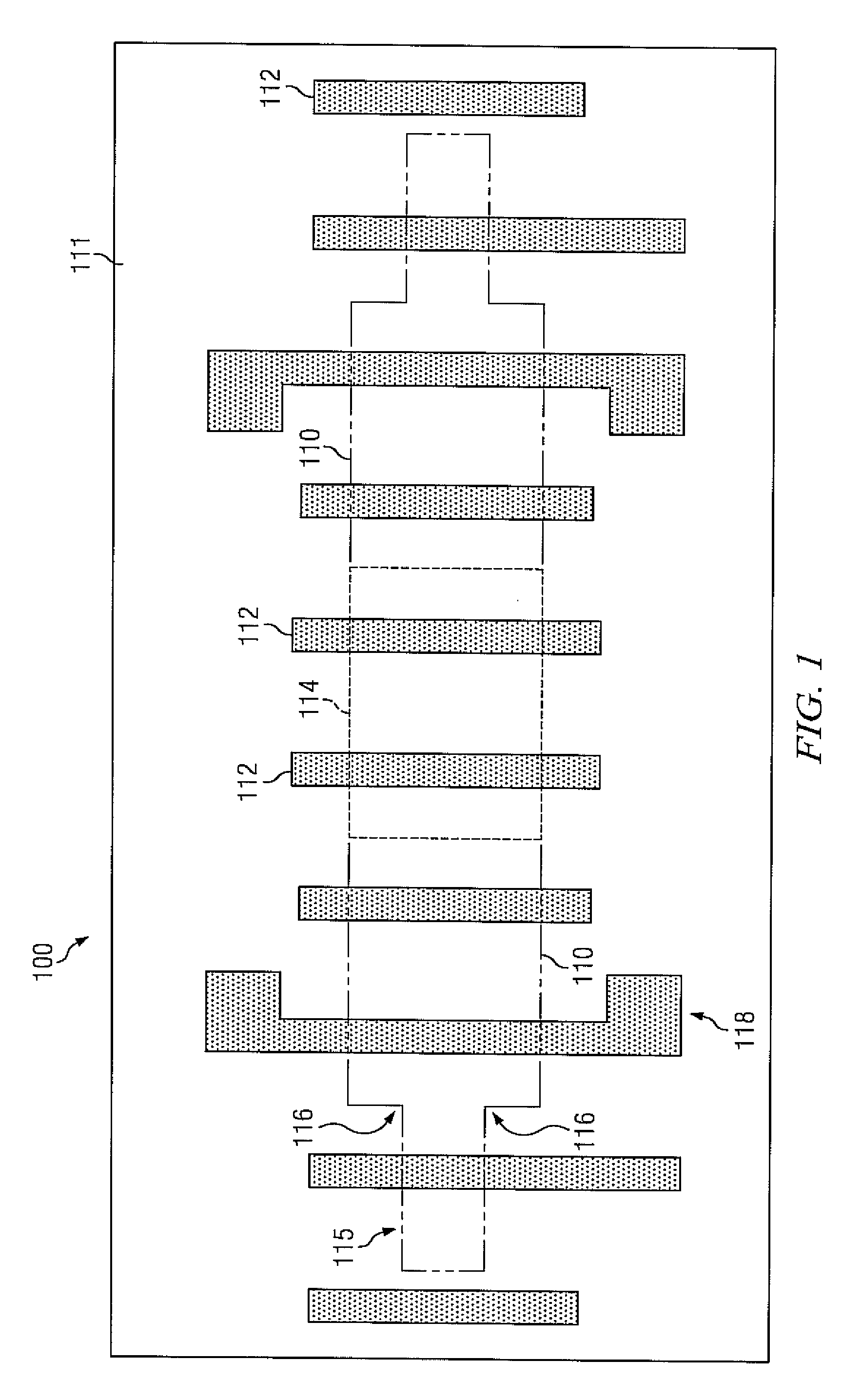
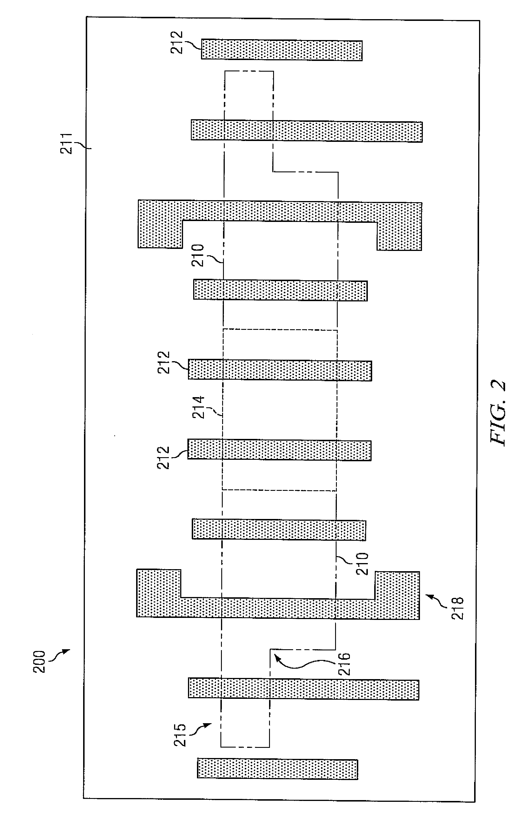
[0026]Reference will now be made in detail to the present embodiments, examples of which are illustrated in the accompanying drawings. Wherever possible, the same reference numbers will be used throughout the drawings to refer to the same or like parts.

[0027]Notwithstanding that the numerical ranges and parameters setting forth the broad scope of the invention are approximations, the numerical values set forth in the specific examples are reported as precisely as possible. Any numerical value, however, inherently contains certain errors necessarily resulting from the standard deviation found in their respective testing measurements. Moreover, all ranges disclosed herein are to be understood to encompass any and all sub-ranges subsumed therein. For example, a range of “less than 10” can include any and all sub-ranges between (and including) the minimum value of zero and the maximum value of 10, that is, any and all sub-ranges having a minimum value of equal to or greater than zero an...


PUM

PropertyMeasurementUnit
sizeaaaaaaaaaa
charge control voltageaaaaaaaaaa

Abstract

In accordance with the invention, there are electron beam inspection systems, electron beam testable semiconductor test structures, and methods for detecting systematic defects, such as, for example contact-to-gate shorts, worm hole leakage paths, holes printing issues, and anomalies in sparse holes and random defects, such as, current leakage paths due to dislocations and pipes during semiconductor processing.

Description

FIELD OF THE INVENTION[0001]The subject matter of this invention relates to fabricating a semiconductor device. More particularly, the subject matter of this invention relates to methods and structures for e-beam testing of systematic and random defects in integrated circuits.BACKGROUND OF THE INVENTION[0002]Competitive yield learning requires defect characterization and rapid resolution of systematic and random defect issues during early integrated circuit development. E-beam testing provides high sensitivity assessment as well as the ability to localize defects for cross-sectioning. Hence, there is a need for E-beam testable structures to characterize known systematic defect issues occurring in, for example, in 45 nm technology, such as contact-to-gate shorts, worm hole leakage paths, contact printing issues, and sparse hole processing.[0003]E-beam has also been used for inspection of random defects such as, dislocations on product wafers and has provided a means of quantifying di...

Claims


Application Information

Patent Timeline
Patent Type & Authority Applications(United States)
IPC IPC(8): G01N23/225G01R31/26
CPCG01R31/2884H01L22/34H01L22/14G01R31/307
Inventor GULDI, RICHARD L.TRAN, TOANRAMAPPA, DEEPAKLYTLE, STEVEN A.
Owner TEXAS INSTR INC
Why Eureka
Try Eureka