Programmable Design Rule Checking

a programming and design technology, applied in the field of programming design rule checking, can solve the problems of increasing the complexity of conventional design rule-checking rules employed by electronic design automation verification tools, the inability to manually design devices, and the physical limitation of polygonal sizes

Inactive Publication Date: 2009-04-23
MENTOR GRAPHICS CORP
View PDF3 Cites 23 Cited by
  • Summary
  • Abstract
  • Description
  • Claims
  • Application Information

AI Technical Summary

Problems solved by technology

Many microdevices, such as integrated circuits, have become so complex that these devices cannot be manually designed.
Moreover, the sizes of the polygons are limited physically by the maximum beam (or beam array) size available to the tool.
Thus, the conventional design-rule-check rules employed by electronic design automation verification tools are becoming more complex as they consider not only single design features, such as wire spacing or gate width, but the interactions of multiple geometric elements in different configurations.
As the number of identified yield loss causes has increased, however, so has the complexity of yield prediction, eventually giving rise to a relatively complex set of design rules.
Another source of complexity is the need for advanced device characterization, where additional device parameters, such as silicon stress or effective gate dimensions, must be extracted to properly analyze the manufacturability of devices.
This diversity in models creates unique challenges for using model-based verification tools.
On the other hand, using a collection of disparate design verification tools for every aspect of a design and manufacturing analysis that may require modeling makes design flow integration much more difficult.
Further, some models may be very specific to a particular design methodology or manufacturing process, or contain sensitive proprietary information, preventing a designer from using commercially available verification tools.

Method used


Image

  • Programmable Design Rule Checking
  • Programmable Design Rule Checking
  • Programmable Design Rule Checking

Examples


Embodiment Construction

Operating Environment

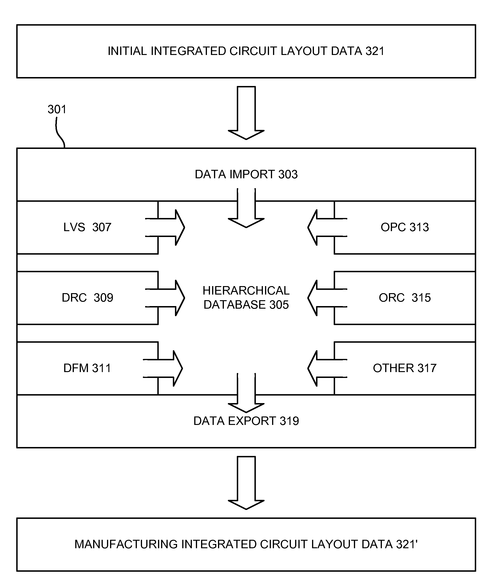
[0026]As will be discussed in more detail below, various embodiments of the invention relate to analog design-rule-check tools for creating and implementing models for various electronic design automation verification processes. With some examples of the invention, an analog design-rule-check tool can be incorporated into a larger electronic design automation verification tool. For still other examples of the invention, an analog design-rule-check tool can be configured as a separate, stand-alone tool. With both arrangements, however, an analog design-rule-check tool according to various embodiments of the invention may be implemented using computer-executable software instructions executable or executed by one or more programmable computing devices.

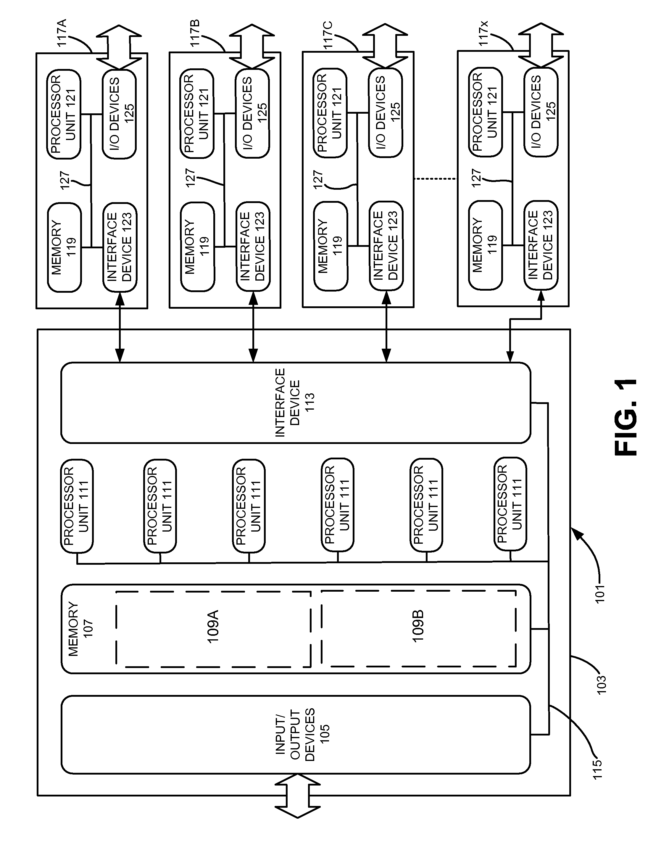
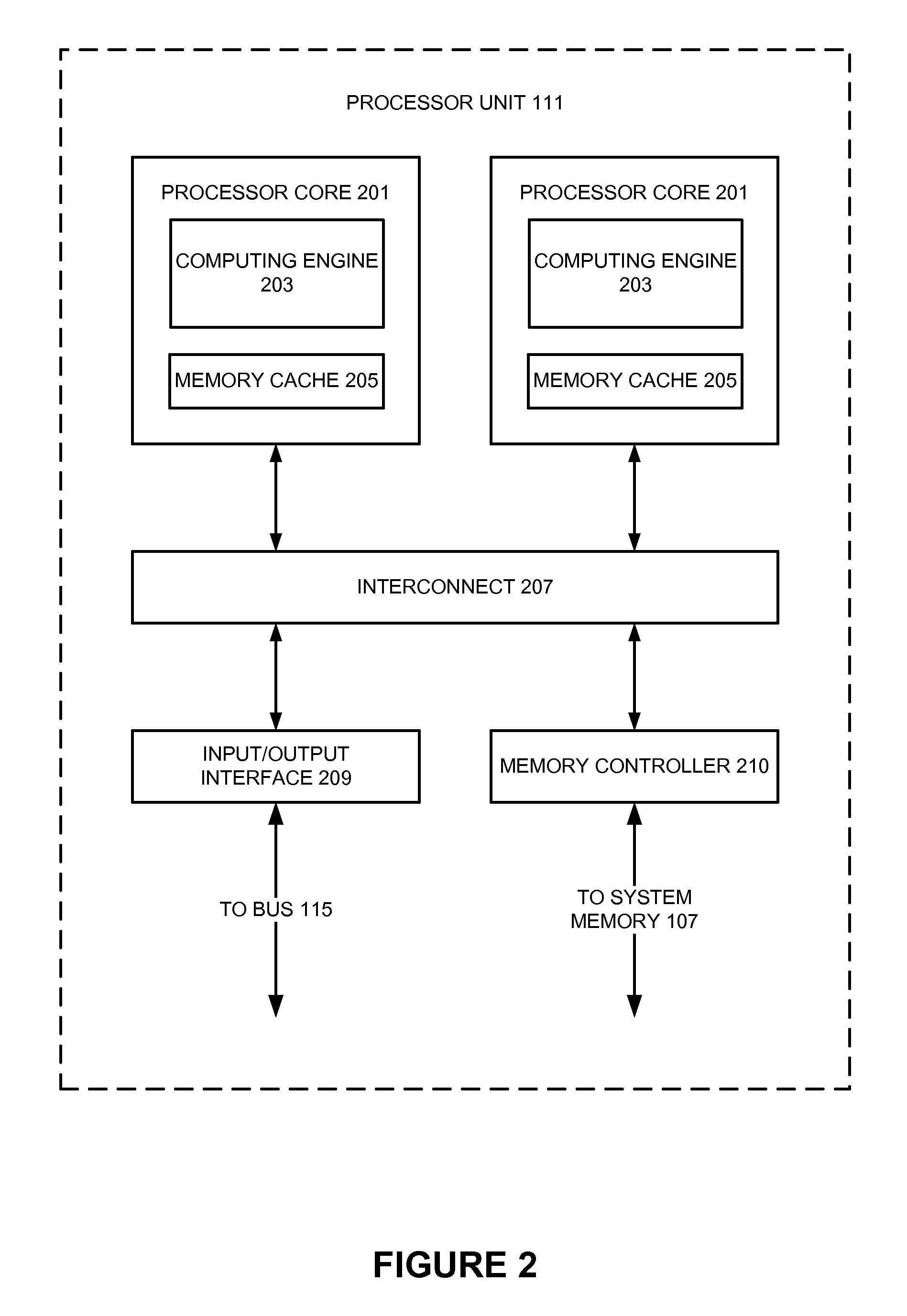
[0027]Because various embodiments of the invention may be implemented using software instructions, the components and operation of a generic programmable computer system on which various embodiments of the invention ...


PUM


Abstract

An analog design-rule-check tool analyzes a microdevice design, such as an integrated circuit design, to identify occurrences of geometric elements that share a specified relationship. When the tool identifies such an occurrence of these geometric elements, it will associate or “cluster” these geometric elements together into an identifiable unit. For specified “clusters” of geometric elements, the analog design-rule-check tool will then determine the value of a measurement or measurements required by a user. Once the analog design-rule-check tool has determined the necessary measurement values, it will use those values to evaluate the function describing a model.

Description

RELATED APPLICATIONS[0001]This application claims priority to U.S. Provisional Patent Application No. 60 / 938,152 entitled “Programmable Design Rule Check Process,” filed May 15, 2007, and naming Fedor G. Pikus as inventor, which application is incorporated entirely herein by reference. This application also claims priority to U.S. patent application Ser. No. 11 / 986,564 entitled “Model-Based Design Verification,” filed Nov. 20, 2007, and naming Fedor G. Pikus et al. as inventors, which in turn claims priority to U.S. Provisional Patent Application No. 60 / 866,579 entitled “Flexible Model-Based DRC And DFM Verification,” filed on Nov. 20, 2006, and naming Fedor Pikus as inventor, which applications are incorporated entirely herein by reference.[0002]In addition, this application claims priority to each of the following patent applications: (1) U.S. Provisional Patent Application No. 60 / 850,716, entitled “Properties In Electronic Design Automation,” filed on Oct. 9, 2006, and naming Fed...

Claims


Application Information

Patent Timeline
Patent Type & Authority Applications(United States)
IPC IPC(8): G06F17/50
CPCG06F17/5081G06F30/398
Inventor PIKUS, FEDOR
Owner MENTOR GRAPHICS CORP
Why Eureka
Try Eureka