Shift register, circuit driving display device, and display device

a display device and shift register technology, applied in the field of shift registers, can solve problems such as phase shift and display quality degradation, and achieve the effects of reducing phase shift signal delay lags, reducing signal delay lags among stages, and reducing signal delay lags

Inactive Publication Date: 2009-05-07
SHARP KK
View PDF6 Cites 9 Cited by
  • Summary
  • Abstract
  • Description
  • Claims
  • Application Information

AI Technical Summary

Benefits of technology

[0011]With this arrangement, a circuit that is same as the shift stopping circuit in configuration is provided in respective stages other than the in-between stage, in which the shift stopping circuit is provided. The circuit is provided in the respective stages other than the in-between stage in such a manner that the circuit does not perform signal processing but serves as a signal path. Making the stages of the shift register uniform in configuration equalizes the signal loads of the stages. This significantly reduces lags (phase shift) in signal delays among the stages. Thus, signal defects resulting from the lags in signal delays among the stages are restrained, so that high-quality display is realized.
[0013]With this arrangement, a circuit that is same as the shift starting circuit in configuration is provided in respective stages other than the in-between stage, in which the shift starting circuit is provided. The circuit is provided in the respective stages other than the in-between stage in such a manner that the circuit does not perform signal processing but serves as a signal path. Thus, signal loads of the stages are equalized so that lags (phase shift) in signal delays among the stages are reduced significantly. Therefore, signal defects resulting from the lags in signal delays among the stages are restrained, so that high-quality display is realized.
[0017]With the foregoing arrangement, signal loads of the stages are equalized so that lags (phase shift) in signal delays among the stages are reduced significantly. Therefore, the signal defects resulting from the lags in signal delays among the stages are restrained, so that high-quality display is realized.
[0022]As the foregoing describes, the shift register of the present invention includes, in respective stages other than the in-between stage in which the shift stopping circuit is provided, a circuit that is provided in such a manner that the circuit does not perform signal processing but serves as a signal path. The circuit is same as the shift stopping circuit in configuration. Making the stages of the shift register uniform in configuration equalizes signal loads of the stages. This significantly reduces lags (phase shift) in signal delays among the stages. Therefore, signal defects resulting from the lags in signal delays among the stages are restrained, so that high-quality display is realized.

Problems solved by technology

Providing the stage of different configuration at a section (in-between section) other than the end sections of the shift register causes the loads to vary, which causes signal defects such as phase shift.
This causes deterioration in display quality.

Method used


Image

  • Shift register, circuit driving display device, and display device
  • Shift register, circuit driving display device, and display device
  • Shift register, circuit driving display device, and display device

Examples


Embodiment Construction

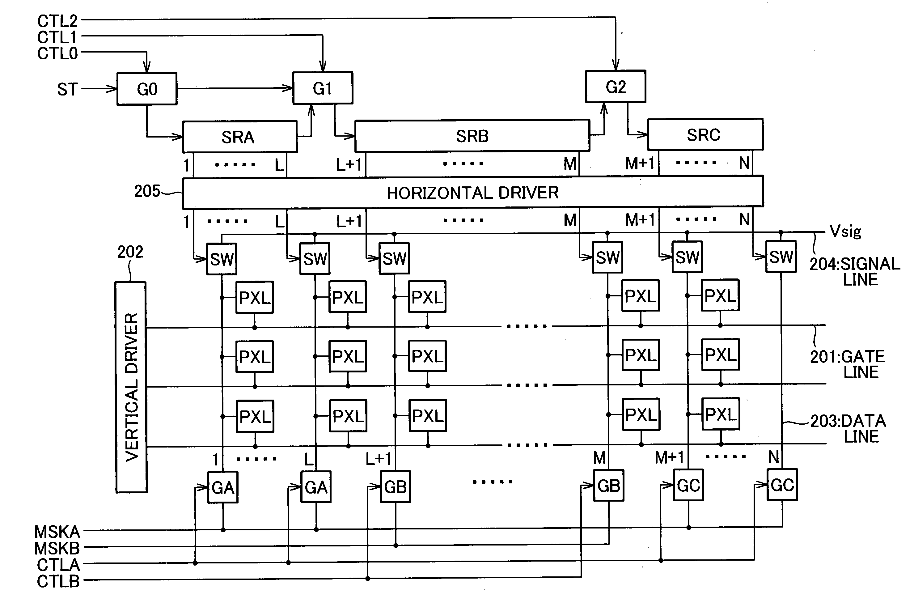
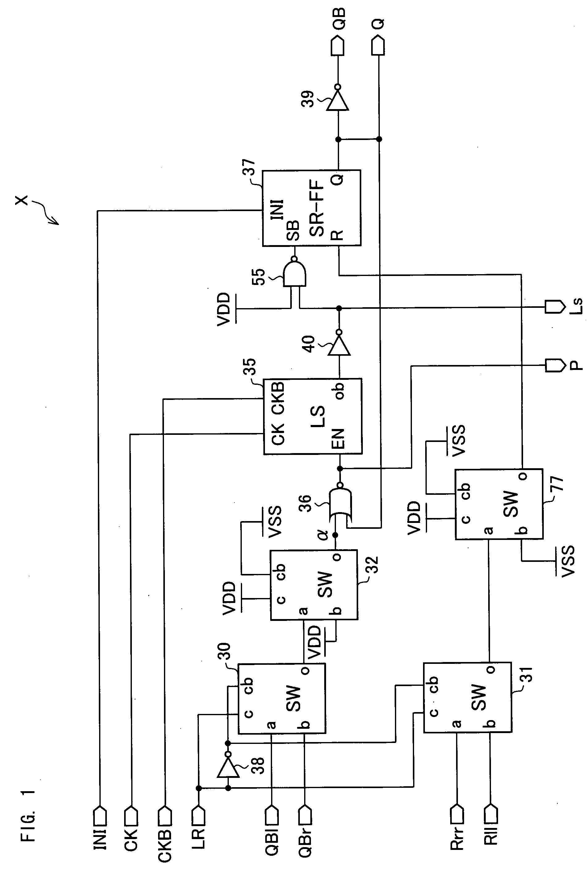
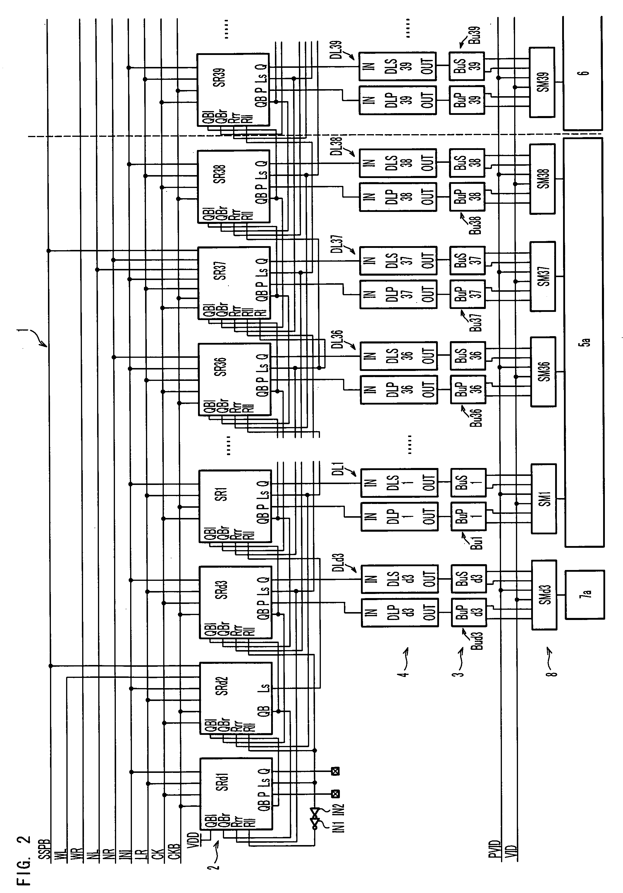
[0122]The following describes an exemplary embodiment of the present invention. FIGS. 2 to 4 are circuit diagrams showing a configuration of a display device 1 of the present embodiment. FIGS. 2 and 3 together correspond to FIG. 4. As showing in those figures, the display device 1 (e.g. liquid crystal display device) includes a source driver and a display section. The source driver includes a shift register 2, a delay circuit section 4, a buffer circuit section 3, sampling circuit section 8, and a mask switch circuit section 9. The display section includes an output line S (Sd3, S1 to S307, and Sd4), a normal-display section 6, wide-display sections (mask section) 5a and 5b, and dummy pixel sections 7a and 7b. Illustration of a configuration of those respective sections and connections between or among those sections are omitted in FIG. 4.

[0123]The shift register 2 includes a plurality of shift register stages (dummy stages SRd1 to SRd3, stages SR1 to SR307, and dummy stages SRd4 to...


PUM


Abstract

In one embodiment of the present invention, the present shift register is a shift register provided in a display device by which a partial-screen display is available. The shift register includes a shift stopping circuit that is provided in an in-between stage, and stops operation of the shift register between a first stage and a last stage of the shift register in partial-screen display. The shift register also includes a circuit that is provided in a stage other than the in-between stage in such a manner that the circuit does not perform signal processing but serves as a signal path. The circuit is same as the shift stopping circuit in configuration. The foregoing allows improvement in display quality of the display device employing the present shift register.

Description

TECHNICAL FIELD[0001]The present invention relates to a circuit that drives a display device such as a liquid crystal display device, and particularly, relates to a shift register thereof.BACKGROUND ART[0002]FIG. 25 is a circuit diagram showing a configuration of a conventional active matrix display device. As shown in this figure, the active matrix display device includes pixels (PXL) arranged in matrix on a horizontally oriented screen. Rows of the pixels are respectively connected to gate lines 201. The gate lines are connected to a vertical driver (vertical driving circuit) 202. On the other hand, columns of the pixels are respectively connected to data lines 203. Further, a signal line 204 is provided to feed a video signal (image signal) Vsig to the pixels. The signal line 4 is connected to the respective data lines 203 via sampling switches SW. The sampling switches operate to open and close sequentially in accordance with a control by a horizontal shift register (SR) via a h...

Claims


Application Information

Patent Timeline
Patent Type & Authority Applications(United States)
IPC IPC(8): G09G3/36
CPCG09G3/3688G09G2310/0232G09G2310/0275G11C19/28G09G2310/0286G09G2310/0289G09G2340/0442G09G2310/0283
Inventor MURAKAMI, YUHICHIROHGYOUTEN, SEIJIROUMATSUDA, NOBORUWASHIO, HAJIME
Owner SHARP KK
Why Eureka
Try Eureka