Electro-optic device and electronic apparatus

a technology of optical devices and electronic devices, applied in optics, instruments, electrical devices, etc., can solve the problems of display devices of related art, image brightness tends to vary, etc., and achieve the effect of uniform image brightness, uniform image brightness, and easy uniformity

Active Publication Date: 2009-05-07
BOE TECH GRP CO LTD
View PDF10 Cites 7 Cited by
  • Summary
  • Abstract
  • Description
  • Claims
  • Application Information

AI Technical Summary

Benefits of technology

[0027]As described above, in this electro-optic device, the first and second pixels have light blocking regions that partially intercept light to be emitted from the respective pixels, the light blocking regions of the first pixel and the second pixel in each pixel group being positioned symmetrically to each other in plan view. Accordingly, the quantity of light reaching the first range from each first pixel through the corresponding opening and the quantity of light reaching the second range from each second pixel through the corresponding opening can be made uniform more readily, whereby the image brightness can be made uniform more readily between the first image and the second image in directional display.
[0028]Because the electronic apparatus according to the second aspect has a display portion defined by an electro-optic device that can make the image brightness uniform more readily between a first image and a second image in directional display, the display portion in the electronic apparatus is capable of making the image brightness uniform more readily between a first image and a second image.

Problems solved by technology

In other words, the display device of the related art is problematic in that the image brightness tends to vary between multiple images in directional display.

Method used


Image

  • Electro-optic device and electronic apparatus
  • Electro-optic device and electronic apparatus
  • Electro-optic device and electronic apparatus

Examples


Embodiment Construction

[0056]A display device, which is an example of an electro-optic device according to an embodiment of the invention, will be described below with reference to the drawings.

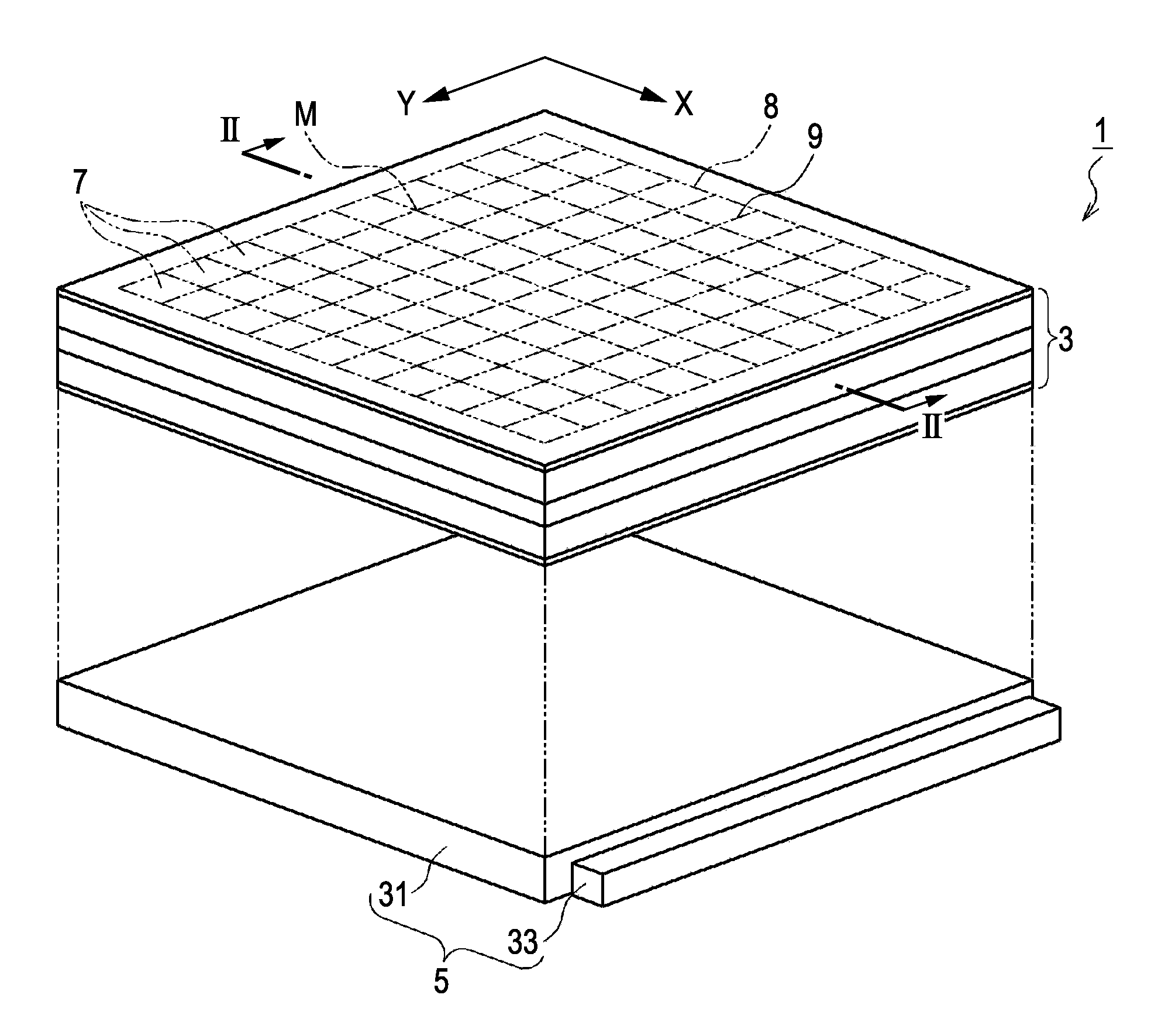
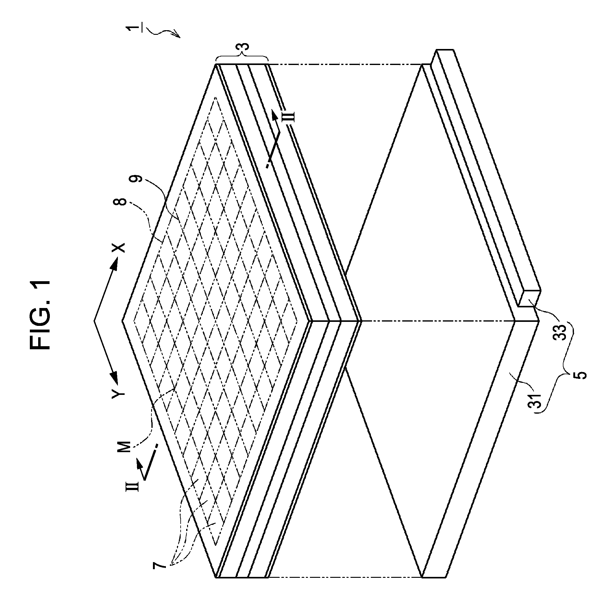
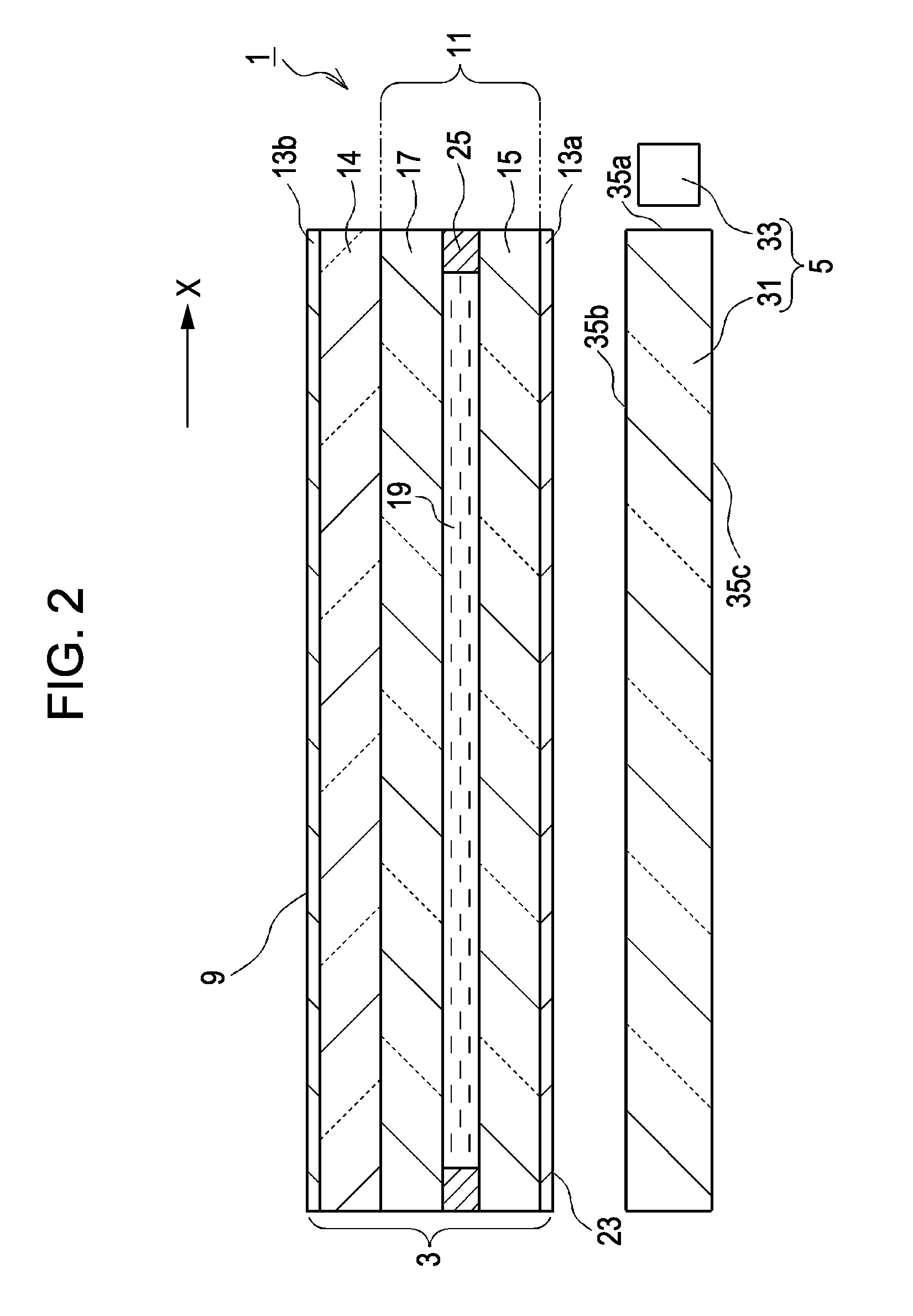
[0057]Referring to FIG. 1, a display device 1 according to an embodiment of the invention includes a display panel 3 and an illuminating unit 5.

[0058]The display panel 3 has a plurality of pixels 7. The pixels 7 are arranged within a display area 8 in an X-axis direction and a Y-axis direction in FIG. 1 so as to form a matrix M, the X-axis direction corresponding to the row direction and the Y-axis direction corresponding to the column direction. In the display device 1, the light from the illuminating unit 5 is received by the display panel 3 and is selectively emitted from the pixels 7 in the display panel 3 through a display face 9, whereby an image can be displayed on the display face 9. The display area 8 is where an image can be displayed. To provide a better understanding of the configuration, the pixels 7 i...


PUM

PropertyMeasurementUnit
peak wavelengthaaaaaaaaaa

Abstract

An electro-optic device includes first and second pixels that form first and second images, respectively. The first and second pixels are arranged alternately in a first direction. A light blocking element overlaps the pixels in plan view. The pixels are divided into pixel groups, each corresponding to every two pixels, which are one of the first pixels and one of the second pixels adjacent to each other in the first direction. The light blocking element has openings, each corresponding to one of the pixel groups and located in a region that overlaps the two pixels of the pixel group in plan view. Each first pixel has a light blocking region that partially intercepts light emitted from the first pixel. Each second pixel has a light blocking region that partially intercepts light emitted from the second pixel. The light blocking regions are positioned symmetrically to each other in plan view.

Description

BACKGROUND[0001]1. Technical Field[0002]The present invention relates to electro-optic devices and electronic apparatuses.[0003]2. Related Art[0004]As an example of an electro-optic device, a display device that can display different images in accordance with various viewing angles is known (such display will be referred to as “directional display” hereinafter). JP-A-2007-108501 (pages 4 to 5 and FIG. 18) discloses an example of a display device of this type that can display different images at various visual points by means of a barrier having openings and light blocking portions.[0005]Regarding a display device having a display panel for forming an image and the aforementioned barrier, the mechanism of how directional display is performed in two directions in the device will be described below with reference to cross-sectional views. Referring to FIG. 25A, a display panel 600 includes a first pixel 601 for displaying a first image and a second pixel 603 for displaying a second ima...

Claims


Application Information

Patent Timeline
Patent Type & Authority Applications(United States)
IPC IPC(8): G02F1/01
CPCG02B27/2214H04N13/0409G02F1/136209G02F1/133524H04N13/31G02F1/1335G02B30/27
Inventor SUGIYAMA, NOBUO
Owner BOE TECH GRP CO LTD
Why Eureka
Try Eureka