Etching method and etching apparatus

a technology of etching apparatus and etching method, which is applied in the direction of electrical equipment, basic electric elements, semiconductor/solid-state device manufacturing, etc., can solve the problems of film peeling in subsequent process steps, and achieve the effect of adjusting the amount of etching more effectively

Inactive Publication Date: 2007-06-14
PANASONIC CORP
View PDF1 Cites 1 Cited by
  • Summary
  • Abstract
  • Description
  • Claims
  • Application Information

AI Technical Summary

Benefits of technology

[0025] Then, the etching can be performed by combining the first and second nozzles in an appropriate manner, which enables the amount of etching to be adjusted more effectively.

Problems solved by technology

However, when the Cu film is formed by the conventional electrolytic plating method, the following problem occurs.
This thick portion of the Cu film formed over the peripheral portion of the semiconductor substrate remains over the semiconductor substrate as a residue, even after a typical chemical mechanical polishing process is performed, and causes film peeling in subsequent process steps.

Method used


Image

  • Etching method and etching apparatus
  • Etching method and etching apparatus
  • Etching method and etching apparatus

Examples


first embodiment

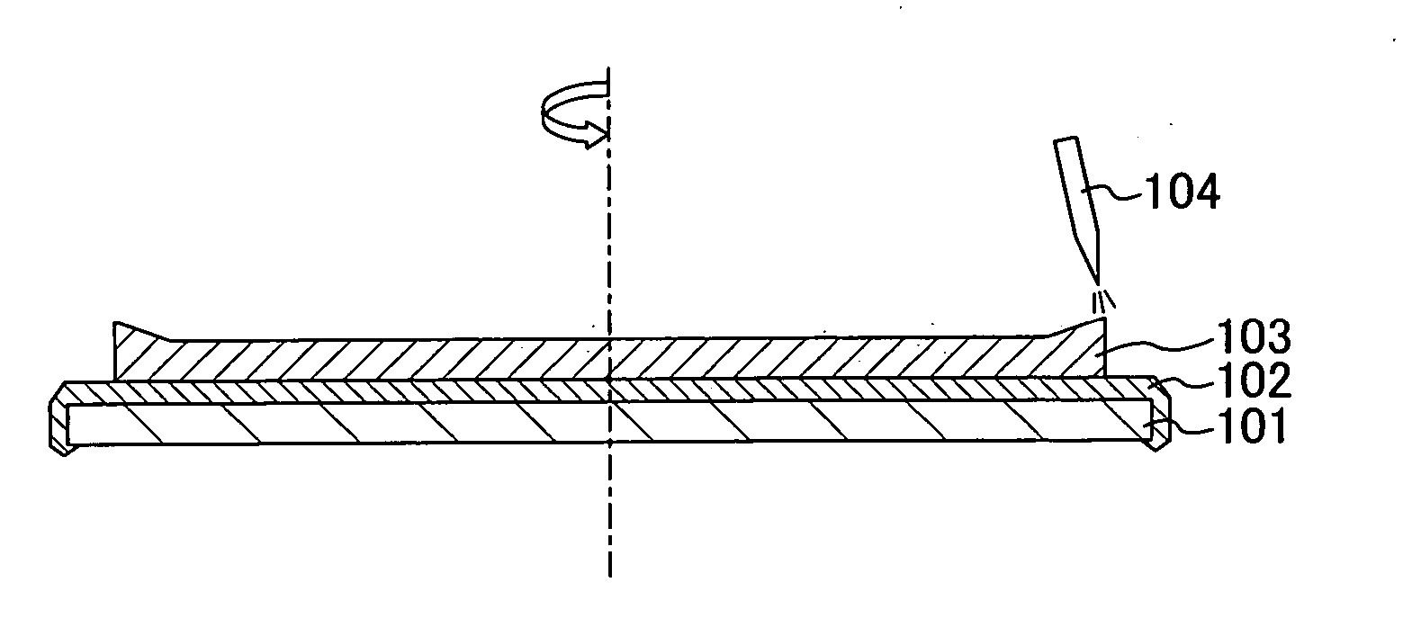
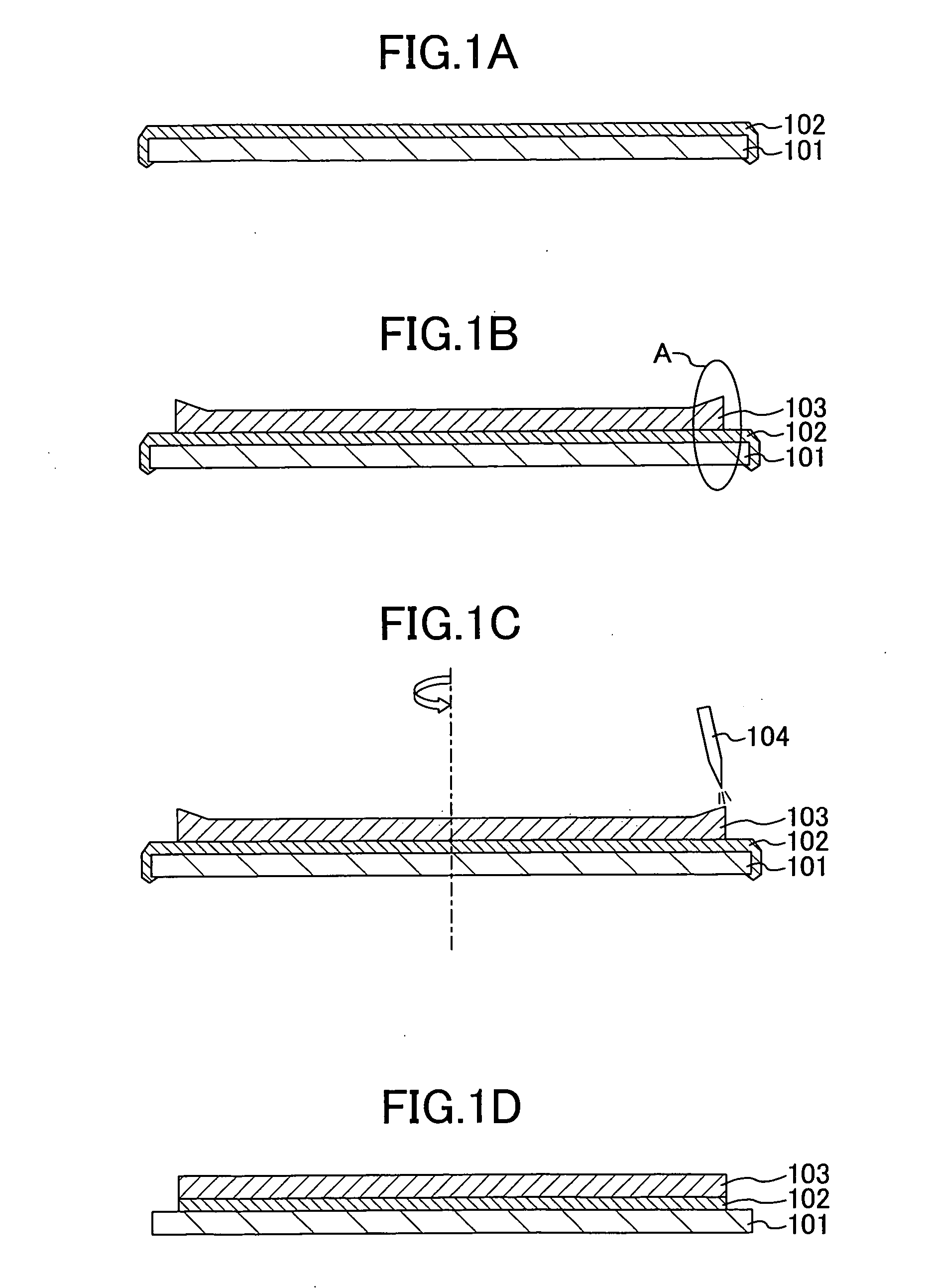
[0037] Hereinafter, a method for etching part of a metal film formed over a peripheral portion of a semiconductor substrate, and an etching apparatus for removing that part of the metal film according to a first embodiment of the present invention will be described.

[0038]FIGS. 1A to 1D are cross-sectional views illustrating a method for etching part of a metal film formed over a peripheral portion of a semiconductor substrate according to the first embodiment of the present invention.

[0039] First, as shown in FIG. 1A, a seed Cu film 102 having a thickness of about 30 nm is formed on a semiconductor substrate 101 by a sputtering process. In this process, the seed Cu film 102 is formed on the side faces of the semiconductor substrate 101 as well.

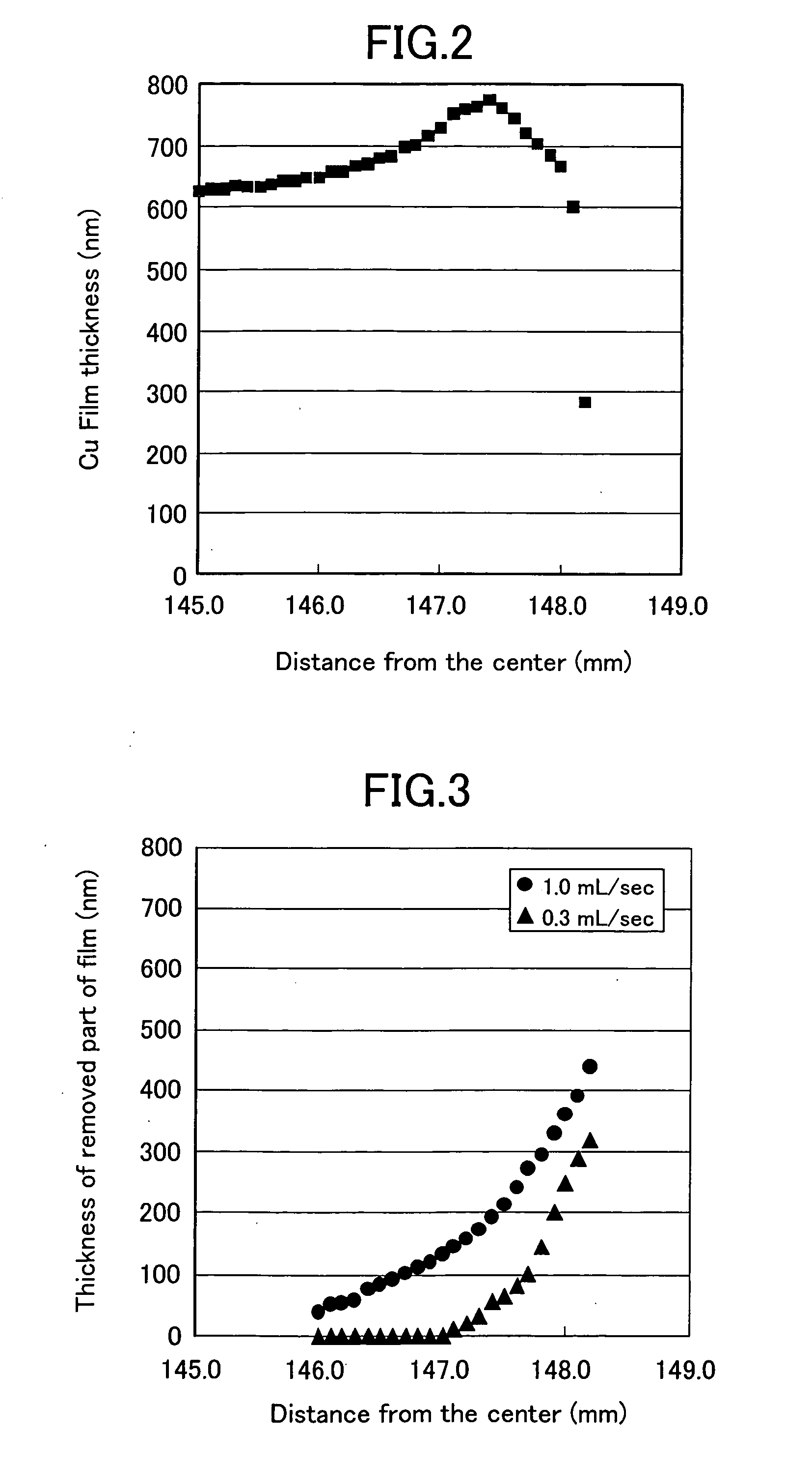
[0040] Next, as shown in FIG. 1B, a Cu film 103 is deposited on the seed Cu film 102 to a thickness of about 600 nm by electrolytic plating. At this time, the Cu film 103 has a larger thickness in a peripheral portion A than in the other po...

second embodiment

[0061] Hereinafter, a method for etching a metal film formed over a semiconductor substrate according to a second embodiment of the present invention will be described.

[0062]FIGS. 5A to 5D illustrate an apparatus for etching a metal film formed over a semiconductor substrate according to the second embodiment of the present invention. FIGS. 5A and 5B are a cross-sectional view and a plan view, respectively, of the etching apparatus in which a nozzle is directed inwardly during etching process. FIGS. 5C and 5D are a cross-sectional view and a plan view, respectively, of the etching apparatus in which the nozzle is directed outwardly during etching process.

[0063] As shown in FIGS. 5A to 5D, the etching apparatus of this embodiment holds a semiconductor substrate 101 and includes a rotatable substrate holder 106, a nozzle 104 for supplying an etching solution, a nozzle rotator 107 for rotating the nozzle 104 to thereby change the angle at which the etching solution is supplied, and a...


PUM

PropertyMeasurementUnit
thicknessaaaaaaaaaa
diameteraaaaaaaaaa
diameteraaaaaaaaaa

Abstract

While a semiconductor substrate having a metal film formed thereover by electrolytic plating is rotated, an etching solution for the metal film is supplied to the peripheral portion of the metal film at a first flow rate and then the etching solution is continuously supplied at a second flow rate, which is lower than the first flow rate.

Description

BACKGROUND OF THE INVENTION [0001] 1. Field of the Invention [0002] The present invention relates to a method for etching part of a metal film formed over a peripheral portion of a semiconductor substrate, and an etching apparatus for removing that part of the metal film. [0003] 2. Description of the Related Art [0004] Conventionally, aluminum (Al) has been mainly used as material of interconnects in LSIs formed on semiconductor substrates made of silicon (Si). In recent years, however, as packaging density on and speed of semiconductor integrated circuits have been increasing, copper (Cu), which has lower resistance than Al and high electromigration (EM) resistance, has been attracting attention as material of interconnects. As a method for forming a Cu film, an electrolytic plating method, which is excellent in filling in trenches and holes, is used. In an electrolytic plating method, a seed Cu film needs to be formed as a seed layer. Therefore, a seed Cu film is formed on the ent...

Claims


Application Information

Patent Timeline
Patent Type & Authority Applications(United States)
IPC IPC(8): H01L21/465C23F1/00
CPCC23F1/00C23F1/08H01L21/02087H01L21/6708
Inventor HIRAO, SHUJI
Owner PANASONIC CORP
Why Eureka
Try Eureka