Method of manufacturing silicon single crystal and silicon single crystal manufactured by the method

a manufacturing method and silicon single crystal technology, applied in the direction of crystal growth process, polycrystalline material growth, under a protective fluid, etc., can solve the problems of deterioration of electrical characteristics, increase of leakage current, and faults in manufactured devices

Active Publication Date: 2007-04-24
SUMITOMO MITSUBISHI SILICON CORP
View PDF4 Cites 0 Cited by
  • Summary
  • Abstract
  • Description
  • Claims
  • Application Information

AI Technical Summary

Benefits of technology

[0008]It is an object of the present invention to provide a method of manufacturing a silicon single crystal ingot wherein the axial temperature gradient in the vicinity of the above-mentioned solid-liquid interface can be made substantially uniform relatively easily, and consequently it is made possible to pull a silicon single crystal ingot in which agglomerates of point defects do not occur in the pulling direction of the silicon single crystal ingot and a perfect region results substantially over the entire length and entire diameter.

Problems solved by technology

The microdefects that become the nuclei of OSF are introduced during crystal growth, and OSF is exposed during a thermal oxidation process or the like in the manufacture of semiconductor devices, causing faults in the manufactured devices, such as an increase in leakage current.
COP becomes a cause of deteriorating electrical characteristics, such as a time dependent dielectric breakdown (TDDB) characteristic and a time zero dielectric breakdown (TZDB) characteristic of oxide films.
In addition, COP existing on a wafer surface can create a height difference in a wiring process of devices, which can become a cause of wire breakage.
Moreover, it becomes a cause of leakage in element-isolating portions, lowering product yield.
This L / D also becomes a cause of deteriorating electrical characteristics, such as leakage characteristics, isolation characteristics, and the like.
For this reason, it has been difficult to manufacture a silicon single crystal ingot that is defect-free over the entire length of the straight cylindrical body of the ingot.

Method used


Image

  • Method of manufacturing silicon single crystal and silicon single crystal manufactured by the method
  • Method of manufacturing silicon single crystal and silicon single crystal manufactured by the method
  • Method of manufacturing silicon single crystal and silicon single crystal manufactured by the method

Examples


example 1

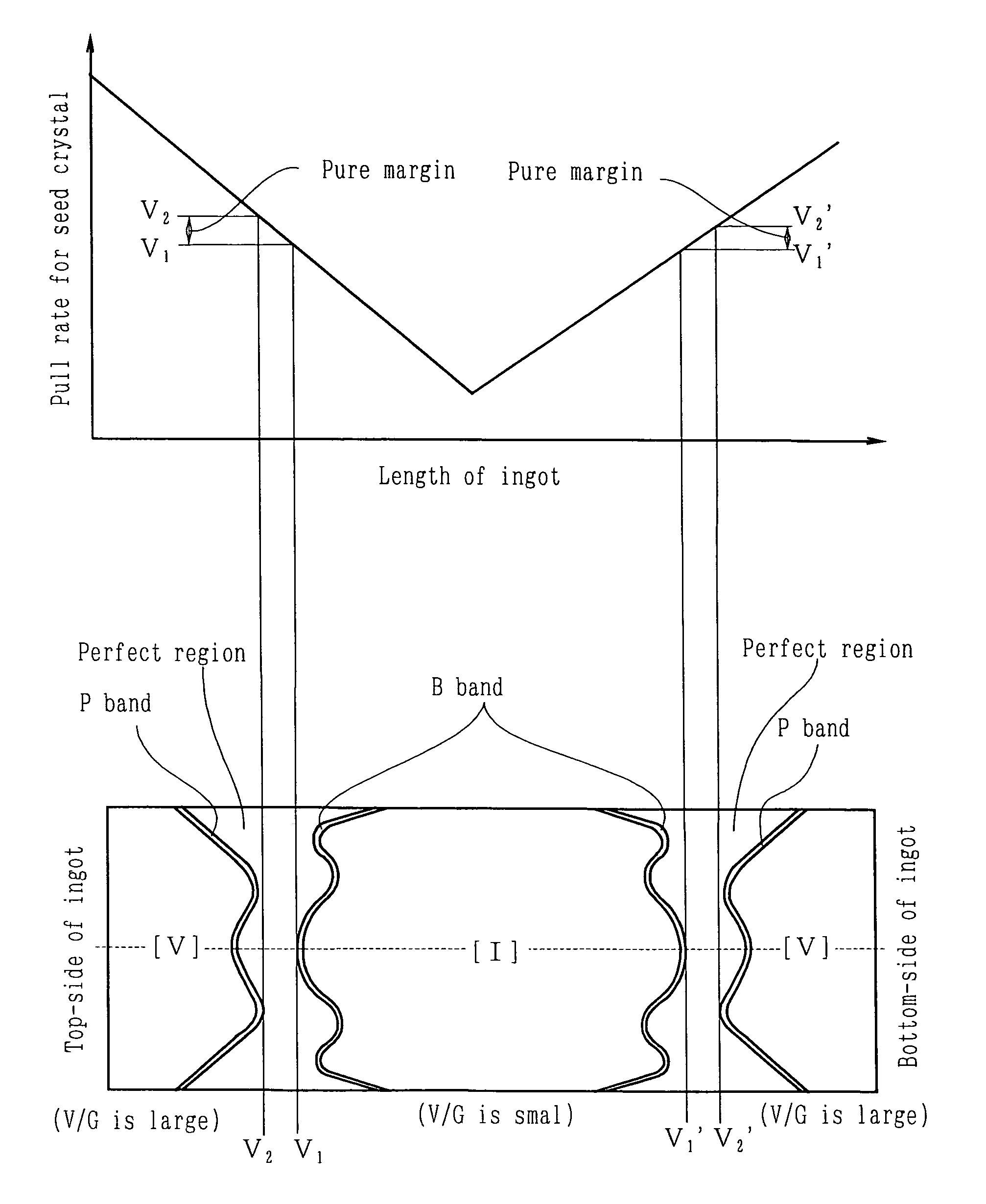
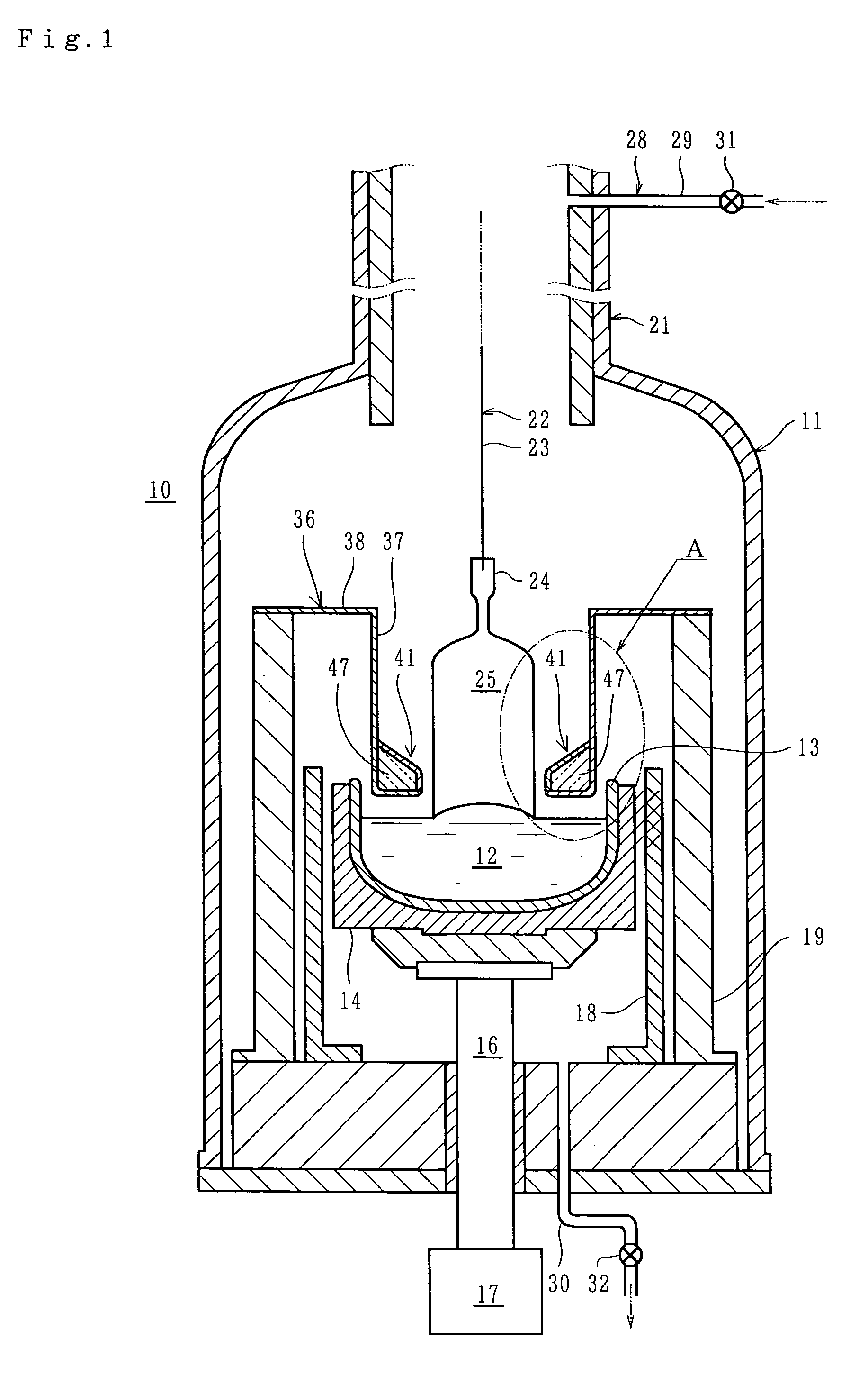
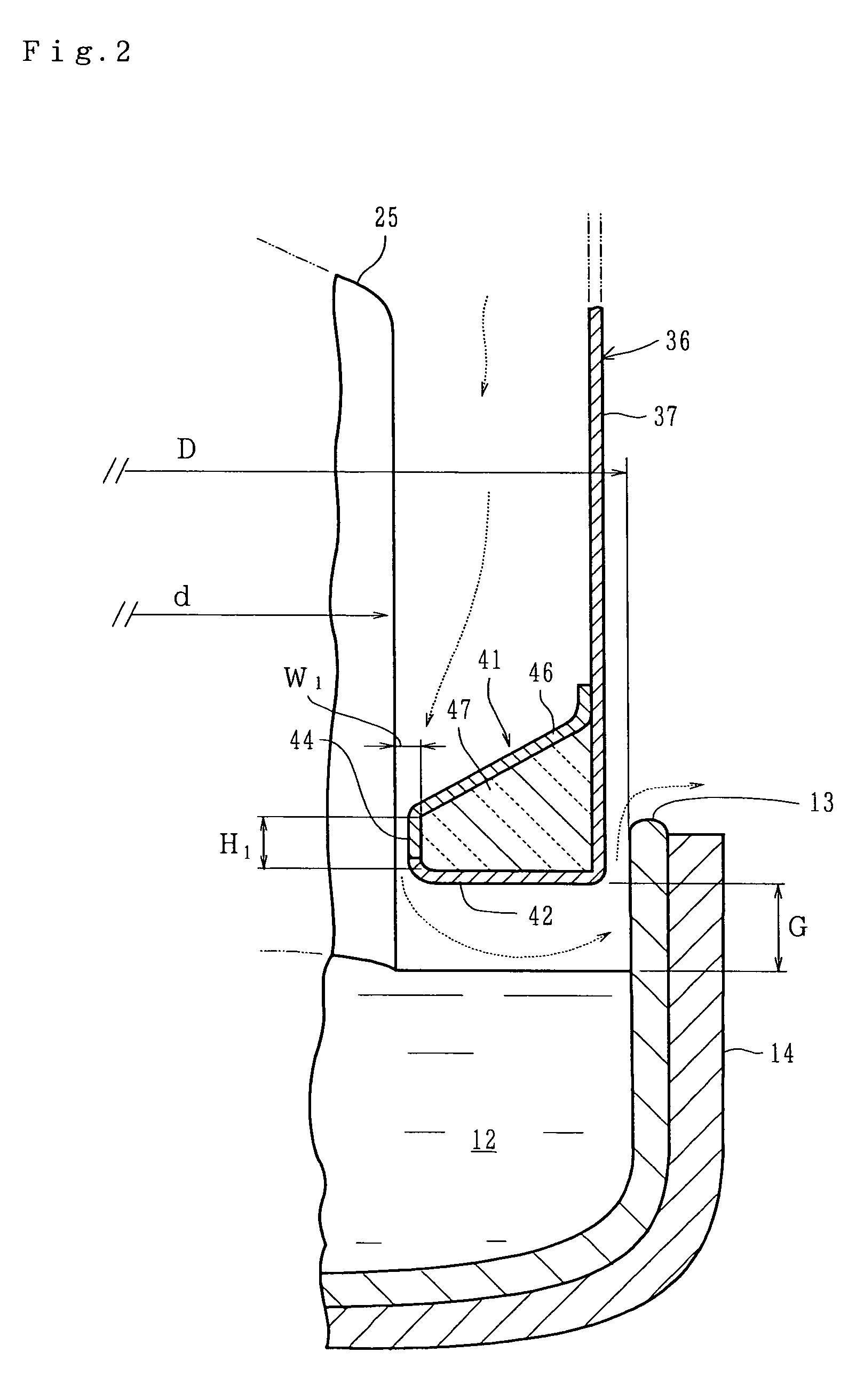
[0045]First, with the use of the pulling equipment 10 shown in FIG. 1, 120 kg poly-silicon (polycrystalline silicon) material was charged, and an ingot 25 having a diameter of about 200 mm was pulled. Next, the rotation speed of the quartz crucible 13 was varied as shown in FIG. 5, whereas the rotation speed of the ingot 25 was made constant, at 18 rpm over the entire length of the ingot, where rotation speeds of the quartz crucible 13 and the ingot 25 during the pulling of the top ingot portion 25a are referred to as CRT and SRT, respectively, and rotation speeds of the quartz crucible 13 and the ingot 25 during the pulling of the bottom ingot portion 25b are referred to as CRB and SRB, respectively. The ingot thus pulled at a predetermined varying pull rate is referred to as Example 1.

example 2

[0046]An ingot was pulled in the same manner as in Example 1 except that the rotation speed of the ingot was varied as shown in FIG. 6. The ingot thus produced is referred to as Example 2.


PUM

PropertyMeasurementUnit
diameteraaaaaaaaaa
flow velocity indexaaaaaaaaaa

Abstract

A silicon single crystal ingot is pulled at a pull rate so that the interior of the ingot results in a perfect region in which agglomerates of interstitial silicon-type point defects and agglomerates of vacancy-type point defects are absent, while rotating a quartz crucible for storing a silicon melt at a predetermined rotation speed and rotating the ingot pulled from the silicon melt in the opposite direction to the rotation of the quartz crucible at a predetermined rotation speed. An average rotation speed CRTAV of the quartz crucible during the pulling of a top ingot portion is set to be faster than an average rotation speed CRTAV of the quartz crucible during the pulling of a bottom ingot portion of the silicon single crystal ingot.

Description

BACKGROUND OF THE INVENTION[0001]This application claims Paris Convention priority of Japanese Application No. 2003-023148 filed Jan. 31, 2003, the entire disclosure of which is hereby incorporated by reference.[0002]The present invention relates to a method of manufacturing a silicon single crystal ingot by pulling it from a silicon melt at a pull rate such that the interior of the silicon single crystal ingot becomes a perfect region. The invention also relates to ingots manufactured by this method.[0003]Conventionally, a method of pulling a silicon single crystal ingot according to a Czochralski method (hereinafter also referred to as a CZ method) has been known as a method of manufacturing silicon single crystal ingots. In the CZ method, a silicon melt stored in a quartz crucible is brought into contact with a seed crystal and the seed crystal is pulled up while rotating the quartz crucible and the seed crystal, whereby a columnar silicon single crystal ingot is manufactured.[00...

Claims


Application Information

Patent Timeline
Patent Type & Authority Patents(United States)
IPC IPC(8): C30B15/20C30B15/00C30B29/06
CPCC30B15/203C30B29/06Y10T117/1072Y10T117/1068C30B15/20
Inventor HARADA, KAZUHIROSUZUKI, YOJIABE, HIDENOBU
Owner SUMITOMO MITSUBISHI SILICON CORP
Why Eureka
Try Eureka