Matrix thermal image sensor with bolometric pixel and method of reducing spatial noise

a thermal image sensor and bolometric pixel technology, applied in the field of matrix thermal image sensors, can solve the problems of affecting the accuracy of thermal image sensors, and causing a great dispersion of responses, so as to reduce or even eliminate spatial noise

Inactive Publication Date: 2009-05-14
COMMISSARIAT A LENERGIE ATOMIQUE ET AUX ENERGIES ALTERNATIVES
View PDF2 Cites 20 Cited by
  • Summary
  • Abstract
  • Description
  • Claims
  • Application Information

AI Technical Summary

Benefits of technology

[0017]The proposal according to the invention is to modify the matrix sensor in a manner which makes it possible to reduce or even eliminate the spatial no

Problems solved by technology

A critical problem encountered with bolometric pixel matrices is the great technological dispersion of the values of the resistors, which induces a great dispersion of the responses in the presence of a uniform thermal illumination.
Because the variation of resistance in the effective range of thermal illumination is barely a few kilohms, it can be conceived that this dispersion of several tens of kilohms at the beginning can be extremely inconvenient; specifically, the signals extracted from the matrix will then represen

Method used


Image

  • Matrix thermal image sensor with bolometric pixel and method of reducing spatial noise
  • Matrix thermal image sensor with bolometric pixel and method of reducing spatial noise
  • Matrix thermal image sensor with bolometric pixel and method of reducing spatial noise

Examples


Embodiment Construction

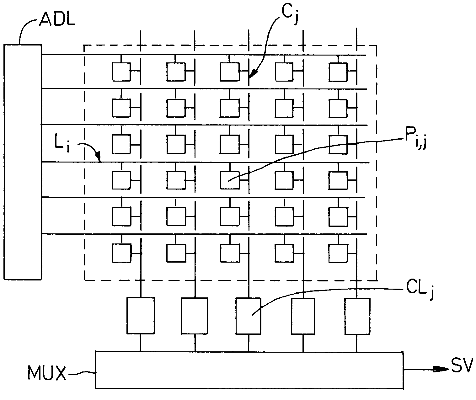
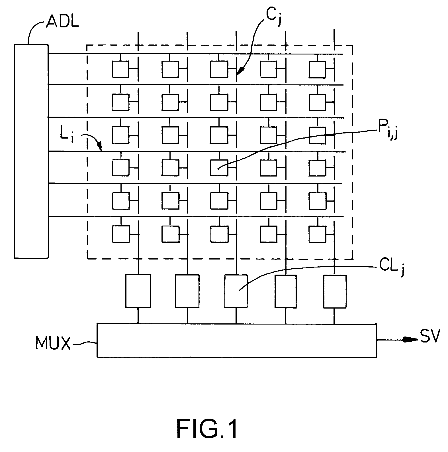
[0043]FIG. 1 shows a very schematic view of the matrix sensor designed to produce a signal representing a thermal image taken by an infrared camera whose sensor is the sensitive element.

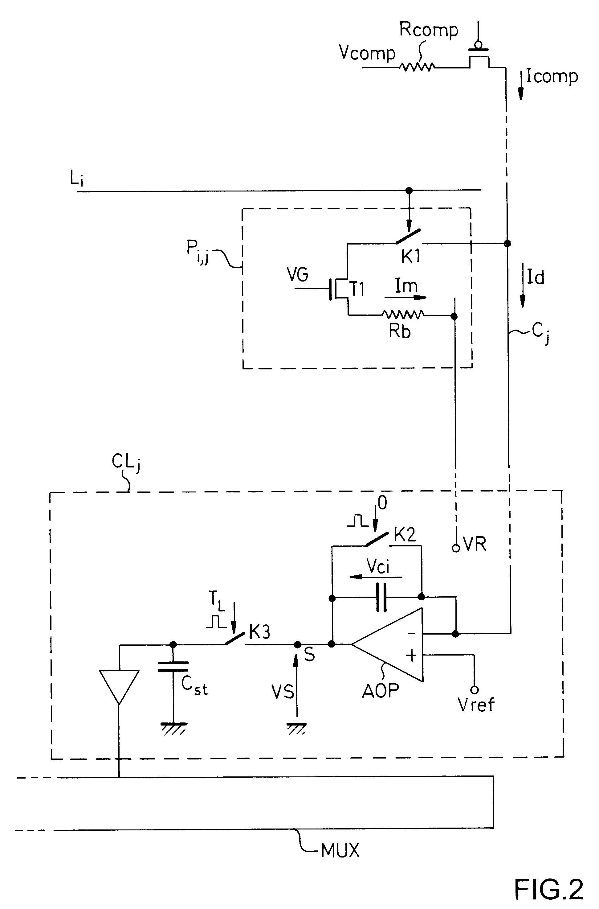
[0044]The sensor comprises a matrix of lines and columns of pixels sensitive to infrared rays. A pixel Pi,j, at the junction of a line of rank i and a column of rank j, is connected to at least one line conductor Li connecting all the pixels of that line and it can be connected to a column conductor Cj connecting all the pixels of that column.

[0045]The line conductor Li is used for addressing the line of pixels; a line addressing circuit ADL successively addresses the various lines of the matrix and the addressing of a line of rank i causes the effective connection of each of the pixels of that line to the column conductor corresponding to that pixel. At the foot of each column, there is a read circuit, indicated by CLj for the column of rank j, which can read a signal applied to the corresponding co...


PUM


Abstract

The invention relates to matrix image sensors of the bolometric type, in which each pixel comprises a bolometric resistor whose value varies according to the thermal flow received by the pixel. The resistor is biased by a bias voltage of value Vpol. The current that passes through it is compensated for by a compensation current Icomp, the difference between these currents being integrated in order to produce a measurement signal. The bias voltage (or the compensation current) is adjusted pixel by pixel, for example during a calibration phase, so that all the pixels have an apparent identical sensitivity despite the dispersion of the nominal value of the bolometric resistor. The adjustment is carried out in an analogue manner by storing an individual voltage specific to each pixel in a sensitivity trimmer capacitor specific to this pixel. The capacitor acts directly on the adjustment of the bias voltage or on other parameters playing a role in the sensitivity of the pixel (integration time for example). The spatial noise is thereby considerably reduced.

Description

RELATED APPLICATIONS[0001]The present application is based on, and claims priority from, French Application Number 07 07418, filed Oct. 23, 2007, the disclosure of which is hereby incorporated by reference herein in its entirety.FIELD OF THE INVENTION[0002]The invention relates to matrix thermal image sensors of the bolometric type, in which each pixel comprises a bolometric resistor whose value varies according to the thermal flow received by the pixel.[0003]The pixels are organized in lines and columns and the matrix can be addressed line by line. A signal read circuit is associated with each column of pixels and there are as many read circuits as there are columns. The signals read on each column during the addressing of a line correspond to the reading of the pixels of this line; they are stored and are then extracted from the matrix by a multiplexer while the reading of the subsequent line begins.BACKGROUND OF THE INVENTION[0004]During the addressing of a line, a bias voltage i...

Claims


Application Information

Patent Timeline
IPC IPC(8): G01J5/02G01J5/00G01J5/03H04N5/365H04N5/3745
CPCG01J5/22H04N5/37452H04N5/3651H04N5/33H04N25/671H04N25/673H04N25/771
Inventor CHAMMING'S, GILLES
Owner COMMISSARIAT A LENERGIE ATOMIQUE ET AUX ENERGIES ALTERNATIVES
Why Eureka
Try Eureka