Film bulk acoustic wave resonator, its fabrication method and film bulk acoustic wave resonator filter using the resonator

a technology of acoustic wave resonator and a fabrication method, which is applied in the direction of piezoelectric/electrostrictive transducers, generators/motors, transducer types, etc., can solve the problems of difficult to obtain good resonance characteristics, and difficult to completely trap a bulk acoustic wave inside the resonator, so as to reduce the connection between th

Inactive Publication Date: 2009-05-21
HITACHI MEDIA ELECTORONICS CO LTD
View PDF5 Cites 64 Cited by
  • Summary
  • Abstract
  • Description
  • Claims
  • Application Information

AI Technical Summary

Benefits of technology

[0016]In accordance with the present invention, the resonance part composed of an upper electrode layer and a lower electrode layer interposing a piezoelectric layer between them is configured in such a way that it is not supported by having the support layer or the piezoelectric layer cover a hollow and that reinforcing props are disposed underneath the reson

Problems solved by technology

However, the following problems are found in film bulk acoustic wave resonators used in radio frequency band as disclosed in Japanese Patent Application Laid-Open Nos. 2006-295380 and 2006-352854, and 1994 IEEE International Frequency Control Symposium, pp.
Since it is difficult to completely get rid of the leakage path of a bulk acoustic wa

Method used


Image

  • Film bulk acoustic wave resonator, its fabrication method and film bulk acoustic wave resonator filter using the resonator
  • Film bulk acoustic wave resonator, its fabrication method and film bulk acoustic wave resonator filter using the resonator
  • Film bulk acoustic wave resonator, its fabrication method and film bulk acoustic wave resonator filter using the resonator

Examples


embodiment 1

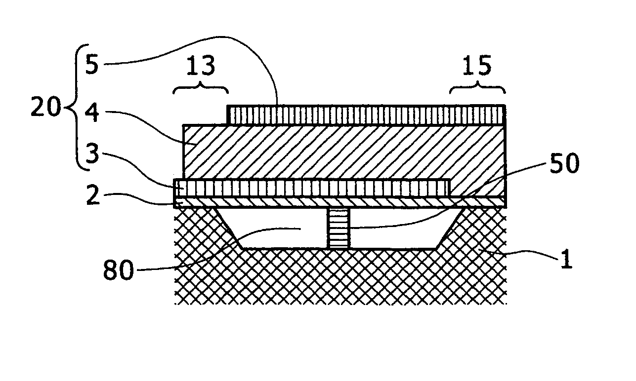
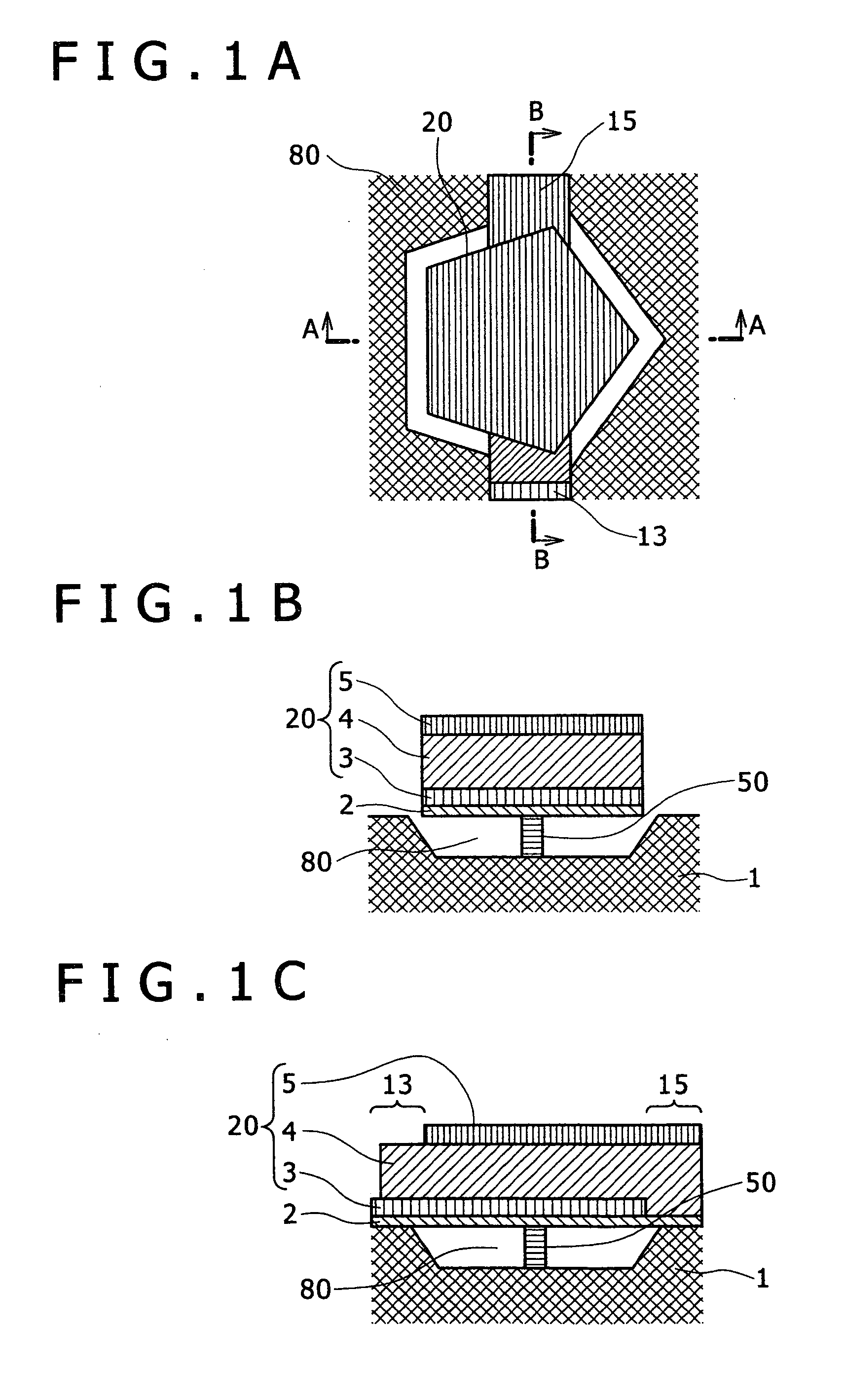
[0034]FIG. 1A is a top schematic view of a film bulk acoustic wave resonator according to a first embodiment, and FIGS. 1B and 1C each show a cross-sectional schematic view of the film bulk acoustic wave resonator according to the first embodiment. In detail, the FIG. 1B is a sectional view taken along line A-A in FIG. 1A, and FIG. 1C is a sectional view taken along line B-B in FIG. 1A. An FBAR-type film bulk acoustic wave resonator is formed on an insulating substrate 1. A laminate-structured resonance part 20 of this FBAR-type film bulk acoustic wave resonator has a laminate structure including a piezoelectric layer 4, and a pair of electrode layers (a first electrode layer 3 and a second electrode layer 5) interposing at least part of the piezoelectric layer 4 between them.

[0035]In the first embodiment of the invention, the insulating substrate 1 is a high-resistance silicon substrate, the first and second electrode layers 3 and 5 are each composed of a molybdenum film obtained b...

embodiment 2

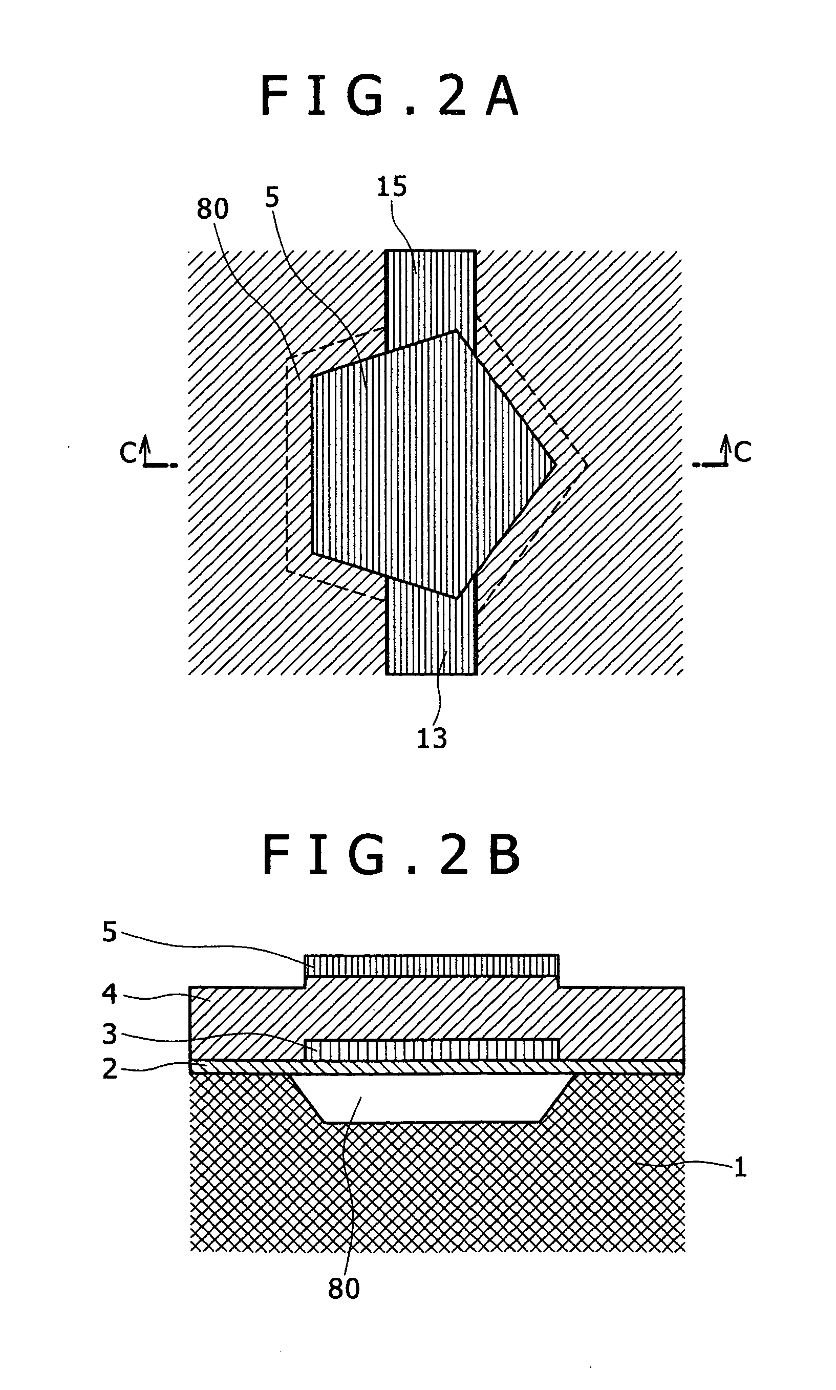
[0047]FIG. 5A is a top schematic view of a film bulk acoustic wave resonator according to a second embodiment, and FIG. 5B is a cross-sectional schematic view of the film bulk acoustic wave resonator according to the first embodiment, which is taken along line D-D in FIG. 5A. Referring to FIGS. 5A and 5B, one example of the film bulk acoustic wave resonator according to the second embodiment of the present invention will be described. In the second embodiment, the film bulk acoustic wave resonator includes a laminate-structured resonance part 20 which is formed on an insulating substrate 1 and composed of a piezoelectric layer 4, a first electrode layer 3 serving as a lower electrode, and a second electrode layer 5 serving as an upper electrode, the first and second electrode layers interposing at least part of the piezoelectric layer 4 between them. The first metal electrode 3 is dispersively formed on an electrode plane facing the second metal electrode 5, and a gap 80 is formed i...

embodiment 3

[0056]FIG. 8A is a top schematic view of a film bulk acoustic wave resonator according to a third embodiment, and FIG. 8B is a cross-sectional schematic view of the film bulk acoustic wave resonator according to the third embodiment, which is taken along line G-G in FIG. 8A. Referring to FIGS. 8A and 8B, one example of the film bulk acoustic wave resonator according to the third embodiment of the present invention will be described. In the third embodiment, the film bulk acoustic wave resonator includes a laminate-structured resonance part 20 which is formed on an insulating substrate 1 and composed of a piezoelectric layer 4, a first electrode layer 3 serving as a lower electrode, and a second electrode layer 5 serving as an upper electrode, the first and second electrode layers interposing at least part of the piezoelectric layer 4 between them. The first metal electrode 3 is dispersively formed on an electrode plane facing the second metal electrode 5, and a gap 80 is formed in t...


PUM

PropertyMeasurementUnit
Diameteraaaaaaaaaa
Areaaaaaaaaaaa

Abstract

The film bulk acoustic wave resonator includes a laminate structure composed of a piezoelectric layer, and first and second electrode layers interposing at least part of the piezoelectric layer, in which the first metal electrode is dispersively formed on an electrode plane facing the second metal electrode, and a gap is formed in a substrate correspondingly to the laminate-structured resonance part. Except for an area of a wire electrode electrically connected to the first electrode layer and an area of a wire electrode electrically connected to the second electrode layer, the piezoelectric layer, first electrode layer and second electrode layer do not come in contact with the insulating substrate but are supported on a hollow. Also, a prop is formed in the gap to support the laminate structure.

Description

CLAIM OF PRIORITY[0001]The present application claims priority from Japanese patent application JP2007-299126 filed on Nov. 19, 2007, the content of which is hereby incorporated by reference into this application.BACKGROUND OF THE INVENTION [0002]1. Field of the Invention[0003]The present invention relates to a resonator using piezoelectric / anti-piezoelectric effects of a piezoelectric layer as well as a resonance phenomenon of a bulk acoustic wave (hereinafter referred to as a “film bulk acoustic wave resonator”), a film bulk acoustic wave resonator filter using such a resonator, and a fabrication method thereof.[0004]2. Description of the Related Arts[0005]In general, a film bulk acoustic wave resonator includes a resonance part having a piezoelectric layer, and first and second metal films, each being obtained by a film forming apparatus, in which the first and second metal films interpose at least part of the piezoelectric layer from above and below. The first metal film serves ...

Claims


Application Information

Patent Timeline
IPC IPC(8): H01L41/00H04R17/00H01L41/09H01L41/187H01L41/22H01L41/29H01L41/332H03H3/02H03H9/05H03H9/17H03H9/54H03H9/70
CPCH03H3/02H03H9/0514H03H9/132Y10T29/42H03H9/173H03H2003/021H03H9/172
Inventor ASAI, KENGOMATSUMOTO, HISANORIISOBE, ATSUSHI
Owner HITACHI MEDIA ELECTORONICS CO LTD
Why Eureka
Try Eureka