Clay Thin Film Substrate, Clay Thin Film Substrate with Electrode, and Display Device Using the Same

Inactive Publication Date: 2009-06-04
TOMOEGAWA CO LTD +1
View PDF2 Cites 13 Cited by
  • Summary
  • Abstract
  • Description
  • Claims
  • Application Information

AI Technical Summary

Benefits of technology

[0021]Since a gas barrier inorganic layer is provided on at least one surface of the clay thin film substrate of the present invention where the clay thin film having a structure, in which oriented clay particles are laminated, it is possible to improve gas barrier properties and to suppress water vapor permeability. In addition, when a planarized inorganic layer is provided for the purpose of surface planarization and stress relaxation, the surface flatness of clay thin films together with the gas barrier properties are improved. Moreover, when an organic polymer layer is provided for the purpose of surface planarization, stress relaxation, and improvements in transparency, the surface smoothness of clay thin films is also similarly improved. Furthermore, the clay thin film substrate of the present invention has equivalent optical properties to those of the plastic substrates used as film substrates for displays. Moreover, the clay thin film substrate of the present invention is also excellent in terms of nonflamability and heat resistance compared to the plastic

Problems solved by technology

Although these displays are excellent compared to the conventional cathode ray tube displays in terms of their mobility and compact size, they are relatively heavy and also break easily, which are their disadvantages, because glass is used as their substrate.
However, for those driven by a thin film transistor (TFT) that are currently mainstream and are capable of dealing with moving images, there are no film substrates available for practical use.
However, there are several problems associated with them when used as a film substrate for liquid crystal and organic EL displays.
One of the problems is surface flatness.
By taking organic EL displays as an example, when the surface of a substrate is not flat, a transparent conductive film cannot be formed uniformly causing reduction in electrical conduc

Method used


Image

  • Clay Thin Film Substrate, Clay Thin Film Substrate with Electrode, and Display Device Using the Same
  • Clay Thin Film Substrate, Clay Thin Film Substrate with Electrode, and Display Device Using the Same
  • Clay Thin Film Substrate, Clay Thin Film Substrate with Electrode, and Display Device Using the Same

Examples


example 1

(1) Production of Clay Thin Film

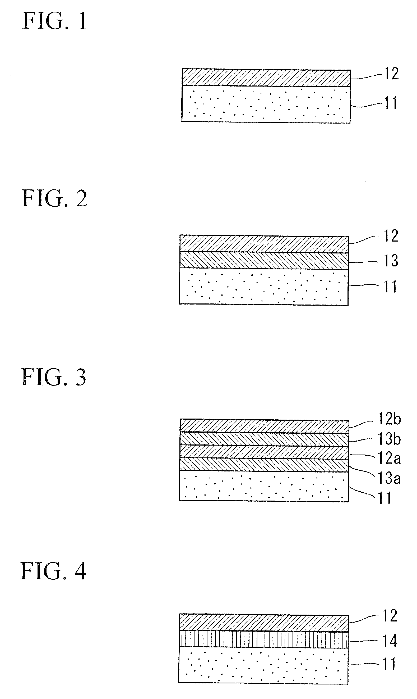
[0075]A clay thin film used as a base was produced by a known method. That is, synthetic smectite was added to distilled water and they were put into a sealed container made of plastic together with a rotor, and the resultant was shaken vigorously to obtain a uniform dispersion. Then, the dispersion was poured into a brass tray, which had a flat bottom face, and the clay dispersion was allowed to stand horizontally to slowly deposit clay particles, and also was dried in a forced draft oven while holding the tray horizontally. A clay thin film having a film thickness of 100 μm was obtained as a result.

(2) Production of Clay Thin Film Substrate

[0076]A gas barrier inorganic layer having silicon oxide as a major component was formed on both sides of the abovementioned clay thin film using a magnetron sputtering apparatus. In other words, the clay thin film was heated to 80° C. in a vacuum chamber and, after removing the residual water content, a gas barri...

example 2

[0079]After producing a clay thin film as in Example 1, a silicon oxide film (a planarized inorganic layer) was formed using a plasma CVD apparatus. In other words, a polymerization reaction was carried out in an oxygen plasma using hexamethyldisiloxane ([(CH3)3Si]2O) as a monomer gas to form a silicon oxide film, which had a film thickness of 200 μm and contained carbon, on both sides of the clay thin film. The average surface roughness Ra was 25 nm before forming the silicon oxide film whereas it was 4 nm after the formation verifying that the surface planarization was achieved. Thereafter, a silicon oxide film (gas barrier inorganic layer), which had a film thickness of 90 nm and contained nitrogen, was formed thereon using the film formation method for gas barrier inorganic layers shown in Example 1 to obtain a clay thin film substrate.

[0080]The water vapor permeability of the clay thin film substrate obtained by the abovementioned method was, under a temperature of 40° C. and a...

example 3

(1) Production of Clay Thin Film

[0084]A clay thin film having a film thickness of 100 μm was obtained as in Example 1.

(2) Production of Clay Thin Film Substrate

(a) Formation of Organic Polymer Layer

[0085]An acrylic, ultraviolet curable resin dissolved in a solvent was coated on the abovementioned clay thin film, and after vaporizing the solvent at 100° C. in a dryer, the resin was cured due to the polymerization using ultraviolet radiation to form an organic polymer layer having a thickness of 2 μm.

(b) Formation of Gas Barrier Inorganic Layer

[0086]A gas barrier inorganic layer having silicon oxide as a major component was formed on the abovementioned clay thin film, where the organic polymer layer was formed, using a magnetron sputtering apparatus. In other words, the clay thin film was heated to 80° C. in a vacuum chamber and, after removing the residual water content, a gas barrier inorganic layer having a film thickness of 90 nm was formed on the abovementioned thin film by the u...


PUM

PropertyMeasurementUnit
Thicknessaaaaaaaaaa
Thicknessaaaaaaaaaa
Temperatureaaaaaaaaaa

Abstract

A clay thin film substrate including a clay thin film having a structure, in which oriented clay particles are laminated; and at least a gas barrier inorganic layer which is laminated on at least one surface of the clay thin film.

Description

TECHNICAL FIELD[0001]The present invention relates to a clay thin film substrate having a structure, in which a inorganic layer is laminated on a clay thin film, a clay thin film substrate with an electrode for a display device, and a display device using them.BACKGROUND ART[0002]Conventional cathode ray tube displays are rapidly being replaced by liquid crystal displays (LCD) due to their mobility and compact size. Furthermore, as a next-generation display, organic electroluminescence (EL) displays that are self-luminous and are excellent in terms of luminosity, brightness, and power consumption are now being produced. Although these displays are excellent compared to the conventional cathode ray tube displays in terms of their mobility and compact size, they are relatively heavy and also break easily, which are their disadvantages, because glass is used as their substrate.[0003]In order to solve these problems, a film substrate (which is called “placell”) is used in some liquid cr...

Claims


Application Information

Patent Timeline
IPC IPC(8): G02F1/1333C09K19/00H01J1/62H05K1/03
CPCC04B35/597Y10T428/1095C04B41/5035C04B41/52C04B2111/00275C04B2111/28C04B2235/963C23C16/401G02F1/133305G02F2001/133302H01L51/52H01L51/5237H01L51/5262C04B41/009Y10T428/1086Y10T428/1055C04B14/106C04B41/4531C04B41/0045C04B41/483C04B41/522C04B41/4533Y02E10/549C09K2323/04C09K2323/061C09K2323/06G02F1/133302H10K77/111H10K50/80H10K50/8445H10K50/85B32B18/00C23C14/06G02F1/1333H10K59/00
Inventor INOUE, TOMOHITOTSUDA, HAJIMEMOTEGI, KATSUMIEBINA, TAKEOMIZUKAMI, FUJIO
Owner TOMOEGAWA CO LTD
Why Eureka
Try Eureka