Shield structure for electronic device

a shield structure and electronic device technology, applied in the direction of magnetic/electric field screening, electrical devices, etc., can solve the problems of ensuring flatness, electromagnetic waves may leak outside the device through gaps, and gaps, so as to prevent effective leakage of electromagnetic waves

Inactive Publication Date: 2009-06-04
PANASONIC CORP
View PDF26 Cites 7 Cited by
  • Summary
  • Abstract
  • Description
  • Claims
  • Application Information

AI Technical Summary

Benefits of technology

[0009]Under these circumstances, it is an object of the present invention to provide a shield structure for an electronic device allowing conductive members to be connected electrically to each other at low impedance while preventing the leakage of electromagnetic waves effectively.
[0011]According to the structure as described above, the protruding portions each are formed between the adjacent through-holes on the laid portion of the first conductive member, and the laid portion of the second conductive member is bent along the surfaces of these protruding portions. Therefore, even between the positions where the first and second conductive members are fastened to each other by the screw members, the protruding portions and the laid portion of the second conductive member are in contact with each other, which ensures the electrical connection between the first conductive member and the second conductive member. As a result, it is possible to prevent effectively the leakage of electromagnetic waves in the areas between the positions where the first and second conductive members are fastened by the screw members. Moreover, each of the protruding portions extends in the direction connecting the adjacent through-holes and the surface thereof is curved smoothly in the longitudinal direction thereof. Therefore, it is possible to bring the protruding portions and the laid portion of the second conductive member into contact in a linear manner along the longitudinal direction of the protruding portions. Accordingly, the present invention makes it possible to connect the first and second conductive members electrically at low impedance while preventing the leakage of electromagnetic waves effectively.

Problems solved by technology

However, gaps are formed between the positions where they are fastened by the screw members, and electromagnetic waves may leak outside the device through the gaps.
It is difficult, however, to ensure the flatness of such frame-shaped surfaces with high accuracy in view of both the workability of the surfaces and the difficulty in keeping the surfaces flat.
Particularly, in many plasma display devices having large frame-shaped surfaces, it is very difficult to ensure the flatness of such large surfaces with high accuracy.
Thus, the impedance between them cannot be lowered sufficiently.

Method used


Image

  • Shield structure for electronic device
  • Shield structure for electronic device
  • Shield structure for electronic device

Examples


Embodiment Construction

[0020]Hereinafter, the preferred embodiments for carrying out the present invention will be described in detail with reference to the accompanying drawings. It should be noted, however, that the embodiments described below are merely exemplary of the present invention, and should not be construed to limit the scope of the present invention.

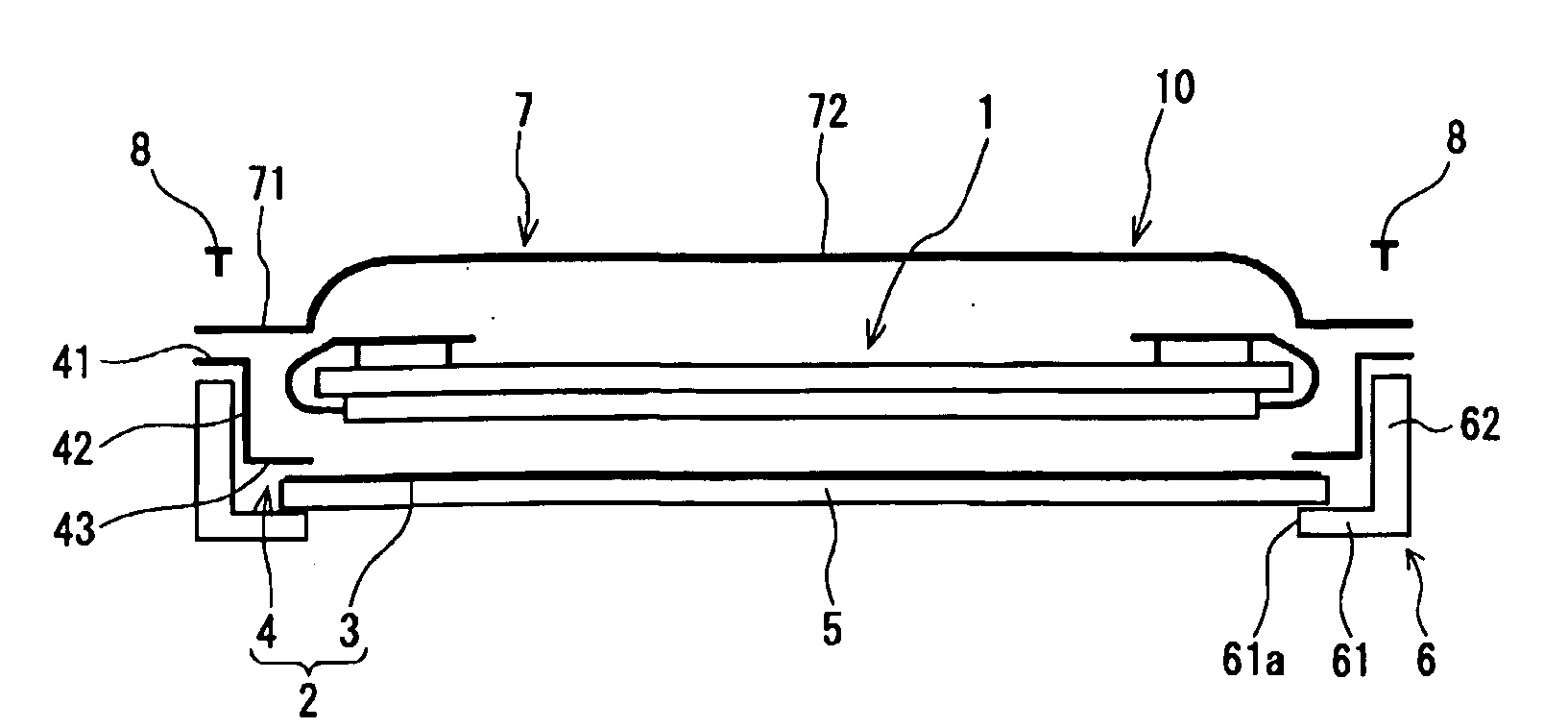
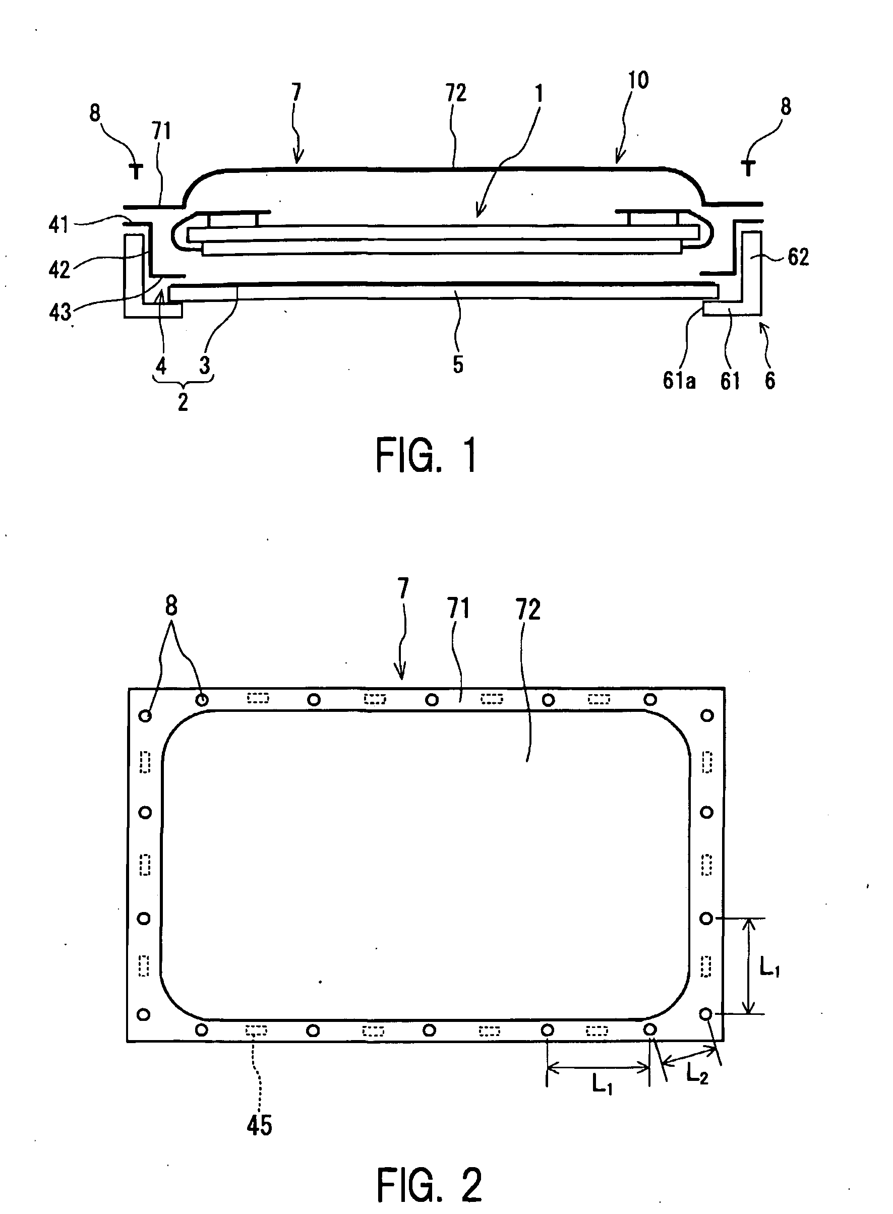
[0021]FIG. 1 is an exploded view of a schematic structure of a plasma display device 10 employing a shield structure for an electronic device according to one embodiment of the present invention. This plasma display device 10 includes: a PDP 1; an EMI (electromagnetic interference) film 3 disposed at the front side of the PDP 1; a transparent substrate 5 that holds the EMI film 3; a frame 6 that covers the front surface of the periphery of the transparent substrate 5; a pressing metal member 4 for pressing the periphery of the transparent substrate 5 against the frame 6 via the EMI film 3; and a back cover 7 disposed at the rear side of the PDP 1....


PUM


Abstract

The present invention provides a shield structure for an electronic device allowing conductive members to be connected electrically to each other at low impedance while preventing the leakage of electromagnetic waves effectively. The first conductive member and the second conductive member for enclosing the electronic device respectively have laid portions that are laid one on the other and fastened to each other at plural positions by means of screw members. Through-holes into which the screw members are to be inserted are formed on both of the laid portions. Protruding portions, which protrude toward the laid portion of the second conductive member, each are formed between the adjacent through-holes on the laid portion of the first conductive member. The protruding portions each have a shape extending in the direction connecting the adjacent through-holes and bulging from both ends toward the center thereof in a smooth curve.

Description

BACKGROUND OF THE INVENTION[0001]1. Field of the Invention[0002]The present invention relates to a shield structure for an electronic device for blocking radiation of electromagnetic waves emitted from the electronic device.[0003]2. Related Background Art[0004]An electronic device such as a plasma display panel (hereinafter referred to as a “PDP”) is equipped with a lot of electronic components that generate electromagnetic waves. In recent years, with the digitization and enhanced performance of electronic devices, unnecessary radiation of electromagnetic waves emitted therefrom has increased. As a countermeasure against these unnecessary electromagnetic waves to ensure the electromagnetic compatibility (EMC), a shield structure in which such an electronic device is enclosed with a conductive member has been proposed.[0005]For example, in a plasma display device including a PDP, a film having a conductive layer is disposed at the front side of the PDP and a conductive back cover is...

Claims


Application Information

Patent Timeline
Patent Type & Authority Applications(United States)
IPC IPC(8): H05K9/00
CPCH05K9/0054
Inventor HAMADA, SEIJIOFUJI, MASAAKIKUBIURA, TAKATOSHIHIROSE, ICHIROFUSAYASU, HIROTSUGUMATSUBARA, RYOICHIKAWA, KEIKUNIMOTO, HIROSHI
Owner PANASONIC CORP
Why Eureka
Try Eureka