Integrated circuits and methods to compensate for defective memory in multiple layers of memory

a technology of integrated circuits and memory, applied in the field of data storage and computer memory, can solve the problems of affecting the use of the inability to use the entire memory array, and the memory density of higher density,

Inactive Publication Date: 2009-06-11
III HLDG 1
View PDF10 Cites 12 Cited by
  • Summary
  • Abstract
  • Description
  • Claims
  • Application Information

AI Technical Summary

Problems solved by technology

Memories having higher densities, however, are vulnerable to increased defect rates (e.g., defects per unit area).
As such, the entire memory array is unusable.
But if the memory is partitioned, the defect will at most affect only the grouping in which the defect resides.
While this approach is functional, it has its drawbacks.
First, extra rows, non-volatile registers, and extra decoders, if used, collectively consume amounts of surface area in traditional memory architectures.
Second, memory designers are typically faced with deciding how many extra memory rows to add to each grouping, especially since memory fabrication processes can randomly cause any number of unforeseen defects.
If a memory designer adds too many extra rows, then any unused memory that does not remedy a

Method used


Image

  • Integrated circuits and methods to compensate for defective memory in multiple layers of memory
  • Integrated circuits and methods to compensate for defective memory in multiple layers of memory
  • Integrated circuits and methods to compensate for defective memory in multiple layers of memory

Examples


Embodiment Construction

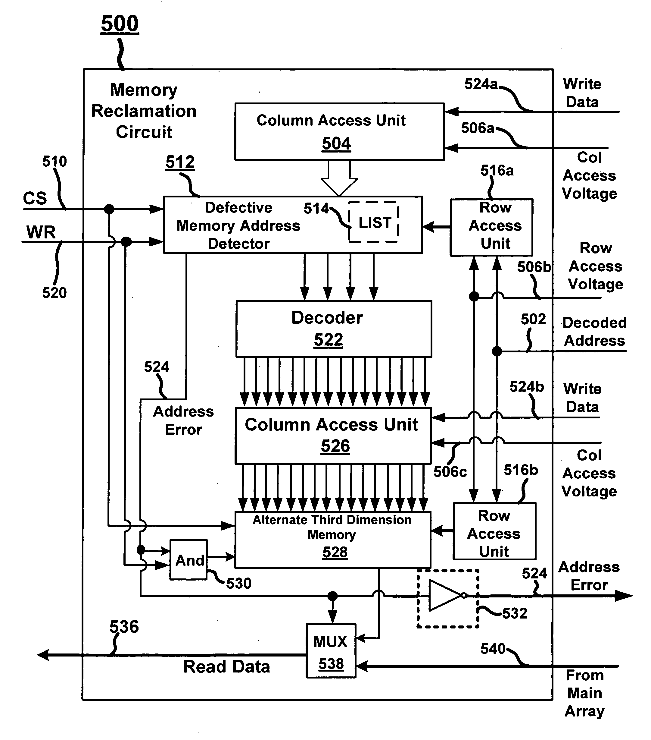
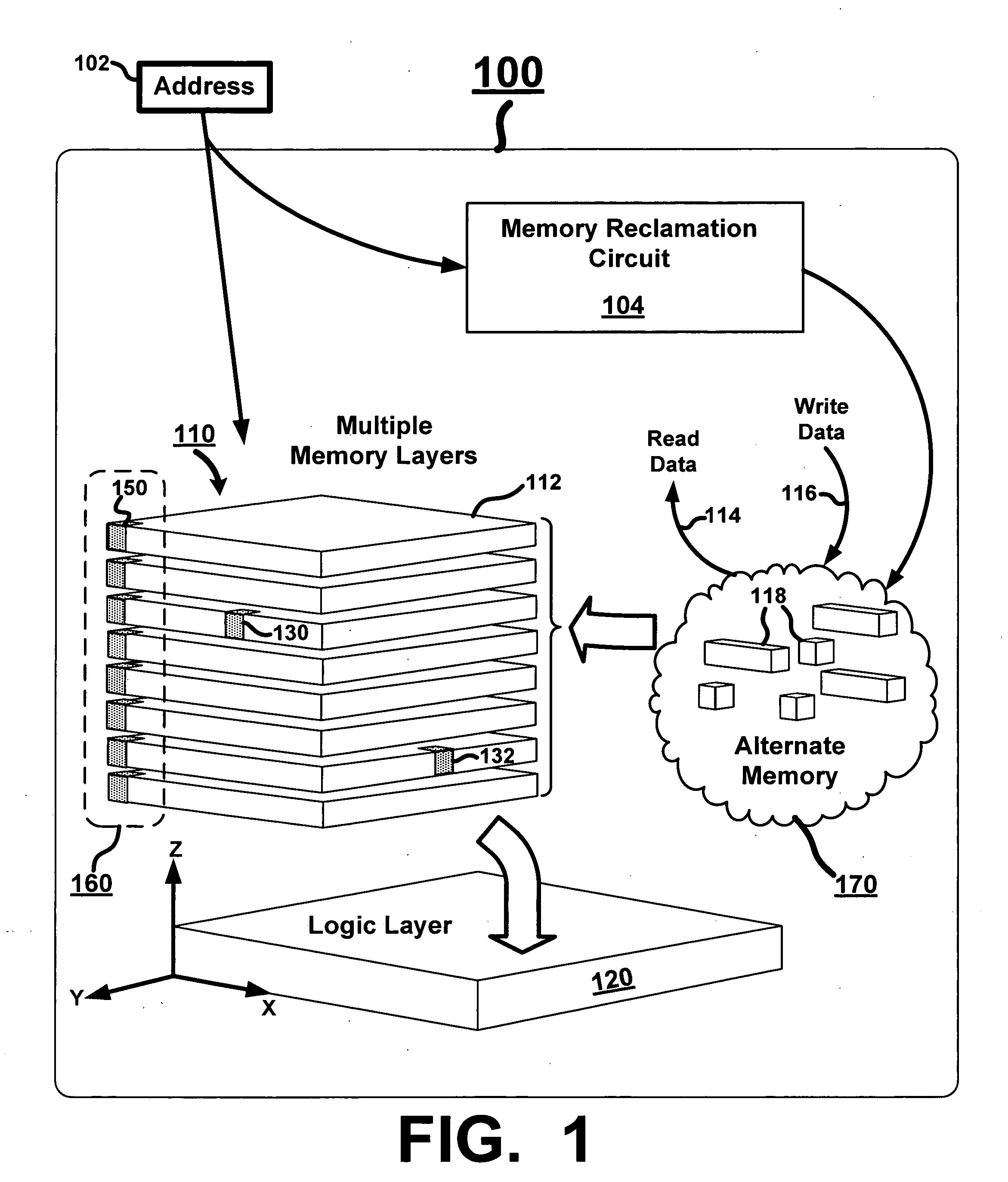
[0017]FIG. 1 illustrates an integrated circuit implementing a memory reclamation circuit configured to compensate for defects in a memory composed of multiple memory layers, according to at least one embodiment of the invention. Integrated circuit 100 includes a memory reclamation circuit 104, a memory 110 including multiple memory layers 112 formed on top of each other (e.g., in the Z dimension), alternate memory 170 and a logic layer 120. Memory 112 is configured to reclaim memory that otherwise would be unavailable due to, for example, defects. As shown, multiple layers of memory 112 can include subsets 118 of alternate memory 170, each including any number of memory cells that operate as substitute memory for defective memory cells. In one embodiment, at least one memory cell in a subset 118 of memory cells can reside in a different plane in memory 110 than at least one defective memory cell. For example, one or more memory cells 132, which form a subset 118 of alternate memory ...


PUM


Abstract

Embodiments of the invention relate generally to data storage and computer memory, and more particularly, to systems, integrated circuits and methods to compensate for defective memory in third dimension memory technology. In a specific embodiment, an integrated circuit is configured to compensate for defective memory cells. For example, the integrated circuit can include a memory having memory cells that are disposed in multiple layers of memory. It can also include a memory reclamation circuit configured to substitute a subset of the memory cells for one or more defective memory cells. At least one memory cell in the subset of the memory cells resides in a different plane in the memory than at least one of the one or more defective memory cells.

Description

CROSS-REFERENCE TO RELATED APPLICATIONS[0001]This application incorporates by reference the following related application: U.S. patent application Ser. No. 11 / 095,026, filed Mar. 30, 2005, and titled “Memory Using Mixed Valence Conductive Oxides,” which has published as U.S. Pub. No. 20060171200.FIELD OF THE INVENTION[0002]Embodiments of the invention relate generally to data storage and computer memory, and more particularly, to systems, integrated circuits and methods for compensating for defective memory in multiple layers of memory implementing, for example, third dimension memory technology.BACKGROUND OF THE INVENTION[0003]Conventional semiconductor fabrication processes have reduced device geometries in the x, y and z directions so as to facilitate the fabrication of relatively dense memory cells. Memories having higher densities, however, are vulnerable to increased defect rates (e.g., defects per unit area). To salvage memory that otherwise would be lost due to defects, memo...

Claims


Application Information

Patent Timeline
IPC IPC(8): G11C29/00
CPCG11C29/808G11C5/02
Inventor NORMAN, ROBERT
Owner III HLDG 1
Why Eureka
Try Eureka