

Electronic component and manufacturing method thereof
a technology of electronic components and manufacturing methods, applied in the direction of printed circuit non-printed electric components association, electrical apparatus construction details, instruments, etc., to achieve the effect of high reliability, high sealability and high sealability
- Summary
- Abstract
- Description
- Claims
- Application Information
AI Technical Summary
Benefits of technology
Problems solved by technology
Method used
Image

Examples
embodiment 1
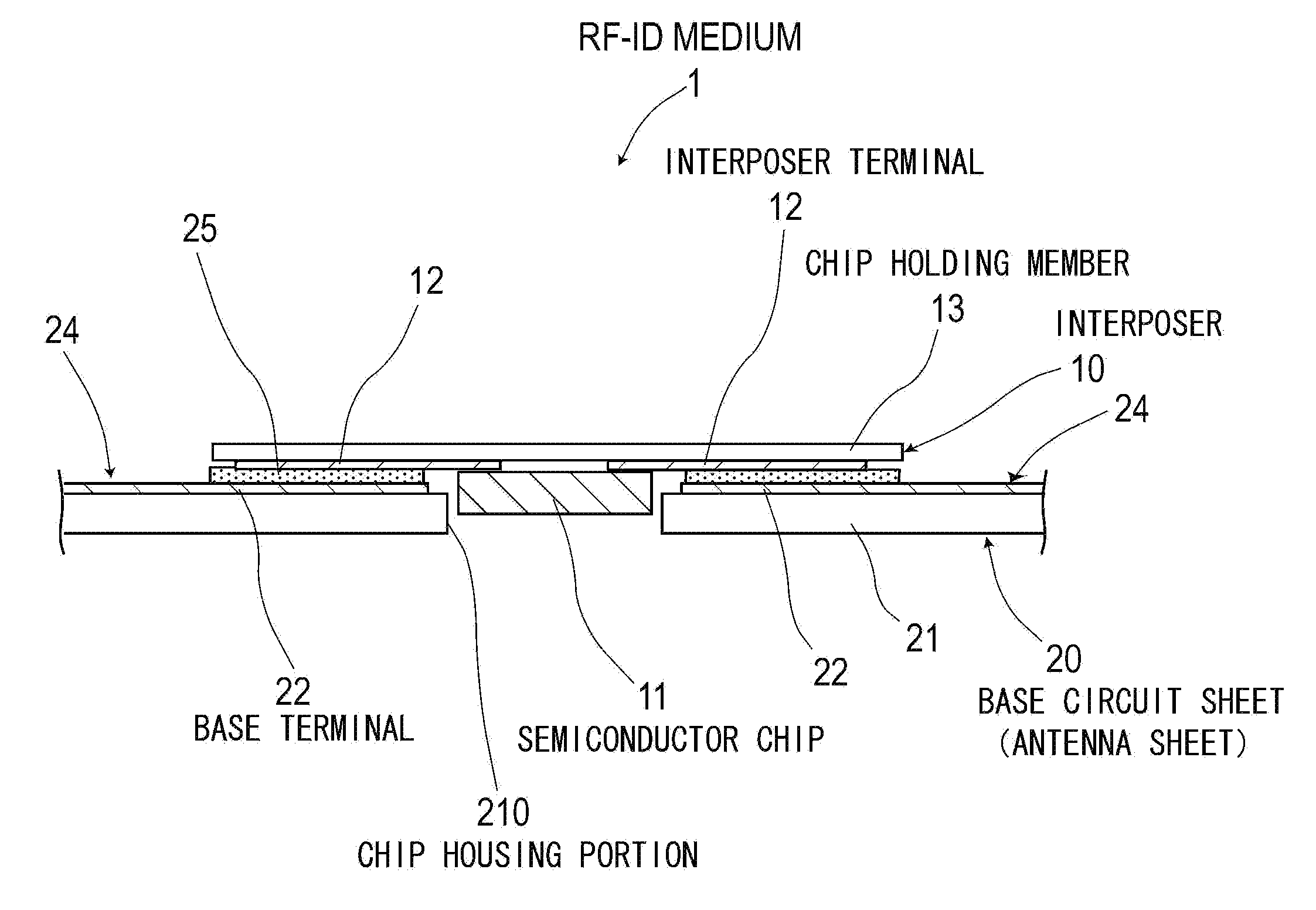
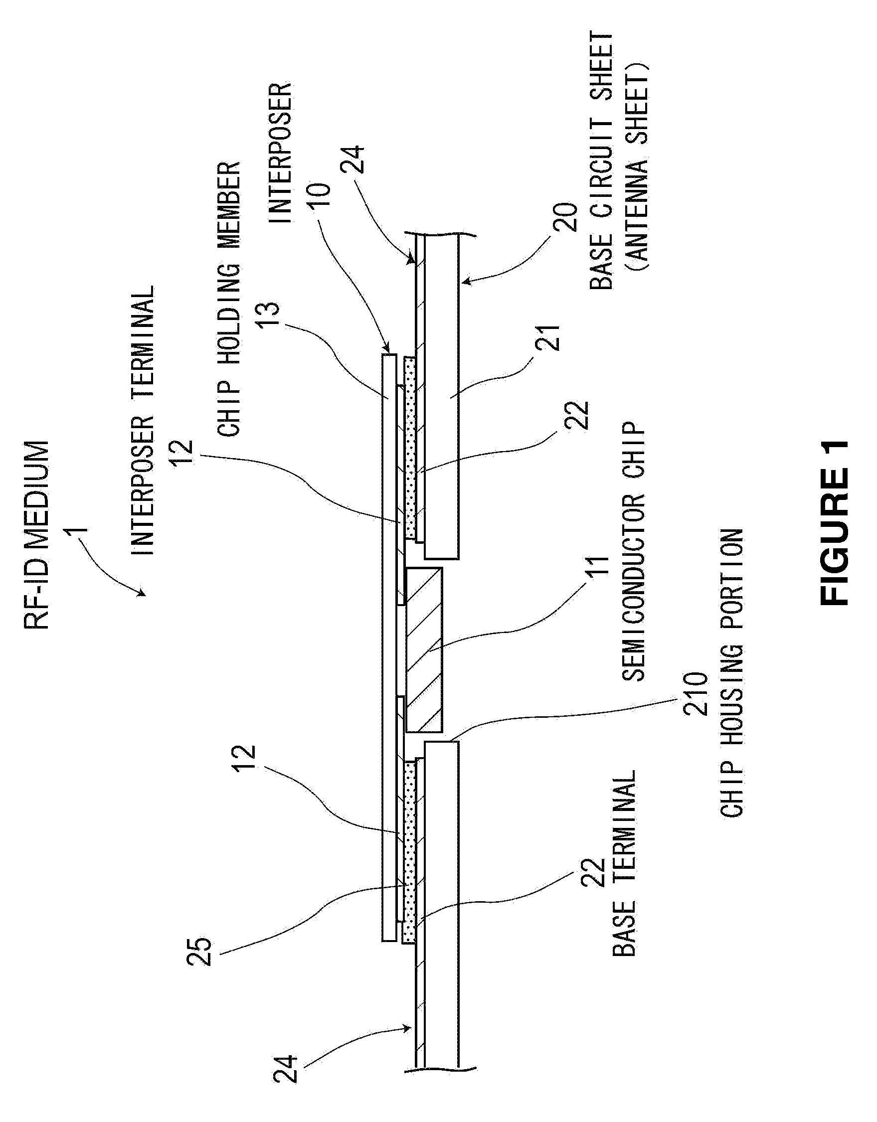
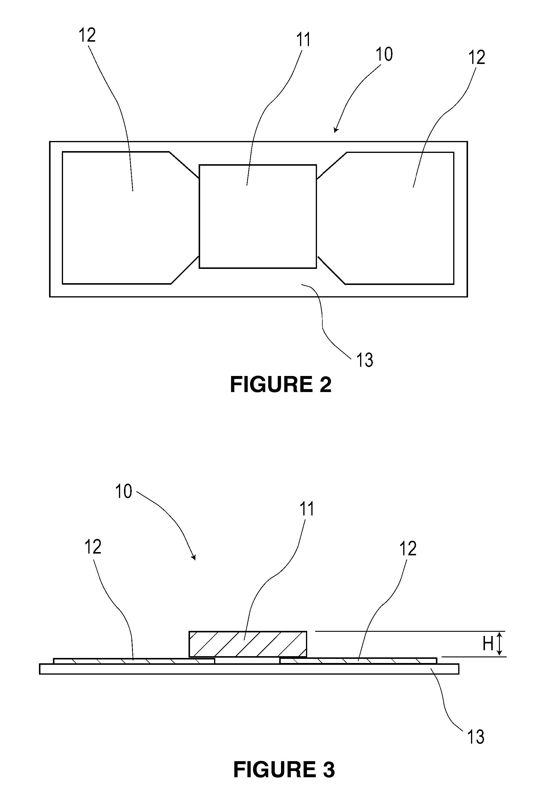
[0051]This embodiment relates to an RFID medium configured using an interposer. This will be described with reference to FIGS. 1 to 6. As shown in FIG. 1, this embodiment relates to an RFID medium that is an electronic component 1 (hereinafter referred to as an RFID medium 1) in which an interposer 10 having a semiconductor chip 11 mounted on a sheet-like chip holding member 13 is bonded to a sheet-like base circuit sheet 20. The interposer 10 has the semiconductor chip 11 mounted on a substantially planar surface of the chip holding member 13, and an interposer terminal 12 that is a conductive pattern electrically extended from a terminal of the semiconductor chip 11. An antenna sheet that is the base circuit sheet 20 (hereinafter referred to as an antenna sheet 20) has a base terminal 22 electrically connected to the interposer terminal 12, and a through chip housing portion 210 for housing the semiconductor chip 11. Now, this will be described in detail.
[0052]As described above, ...
embodiment 2
[0065]This embodiment is such that the chip housing portion 210 is changed to a recessed chip housing portion 210 based on the RFID medium in Embodiment 1, and an insulating adhesive 26 having electrical insulating properties is used as an adhesive. In a stacking step of the embodiment, the insulating adhesive 26 (FIG. 10) is used instead of the conductive adhesive in Embodiment 1. An adhesive providing area 261 is provided so as to substantially match a stacking area of an interposer 10 on a surface of an antenna sheet 20 (FIG. 9). The closed-end recessed chip housing portion 210 is formed. Further, in a bonding step of the embodiment, a press die 31 (FIG. 12) having protrusions 311 on a pressing surface is used to protrudingly deform the antenna sheet 20, thereby ensuring an electrical connection state between the interposer 10 and the antenna sheet 20 (FIGS. 12 to 14). This will be described with reference to FIGS. 8 to 14.
[0066]In a housing portion forming step in the embodiment...
embodiment 3
[0079]This embodiment is such that positioning reliability of the interposer 10 and the antenna sheet 20 is increased based on the RFID medium in Embodiment 1. This will be described with reference to FIGS. 15 and 16. As shown in FIG. 15, an interposer 10 in the embodiment has a protruding engaging portion 115 adjacent to an IC chip 11. An antenna sheet 20 in the embodiment has a through-hole-shaped engaged portion 215 adjacent to a chip housing portion 210. When the interposer 10 and the antenna sheet 20 are stacked, the engaging portion 115 and the engaged portion 215 fit each other. FIG. 15 shows the IC chip 11 deformed in size, and shows a gap between an outer edge of the chip housing portion 210 and the IC chip 11 in a relatively smaller scale than an actual scale.
[0080]The interposer 10 in the embodiment is configured so that the engaging portion 115 and the engaged portion 215 fit each other only when the interposer 10 is mounted to the antenna sheet 20 in a proper direction....
PUM
 Abstract
Description
Claims
Application Information