Construction methods for backside illuminated image sensors

a construction method and image sensor technology, applied in the direction of semiconductor/solid-state device details, electrical devices, semiconductor devices, etc., can solve the problems of insufficient unsatisfactory reduction of light loss and optical crosstalk, and loss of incident ligh

Inactive Publication Date: 2009-07-09
APTINA IMAGING CORP
View PDF17 Cites 144 Cited by
  • Summary
  • Abstract
  • Description
  • Claims
  • Application Information

AI Technical Summary

Problems solved by technology

Some amount of incident light may be lost due to absorption and reflection of incident light in the interconnect structures.
Additionally, some amount of light intended for a given pixel may end up in neighboring pixels due to diffraction and reflection, creating undesirable optical crosstalk between the pixels.
Microlenses, however, may not sufficiently reduce the light loss and optical crosstalk and may be complex to design and manufacture.

Method used


Image

  • Construction methods for backside illuminated image sensors
  • Construction methods for backside illuminated image sensors
  • Construction methods for backside illuminated image sensors

Examples


Embodiment Construction

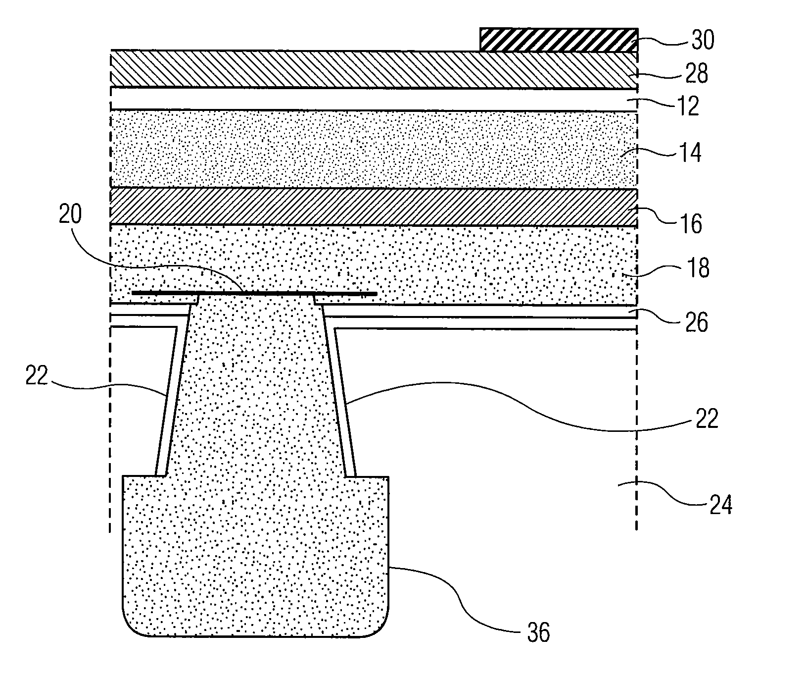
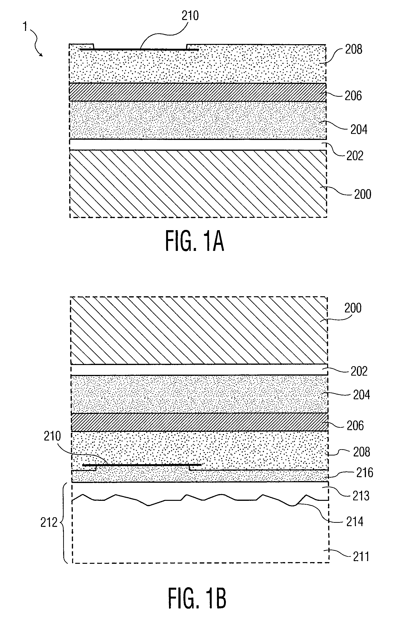
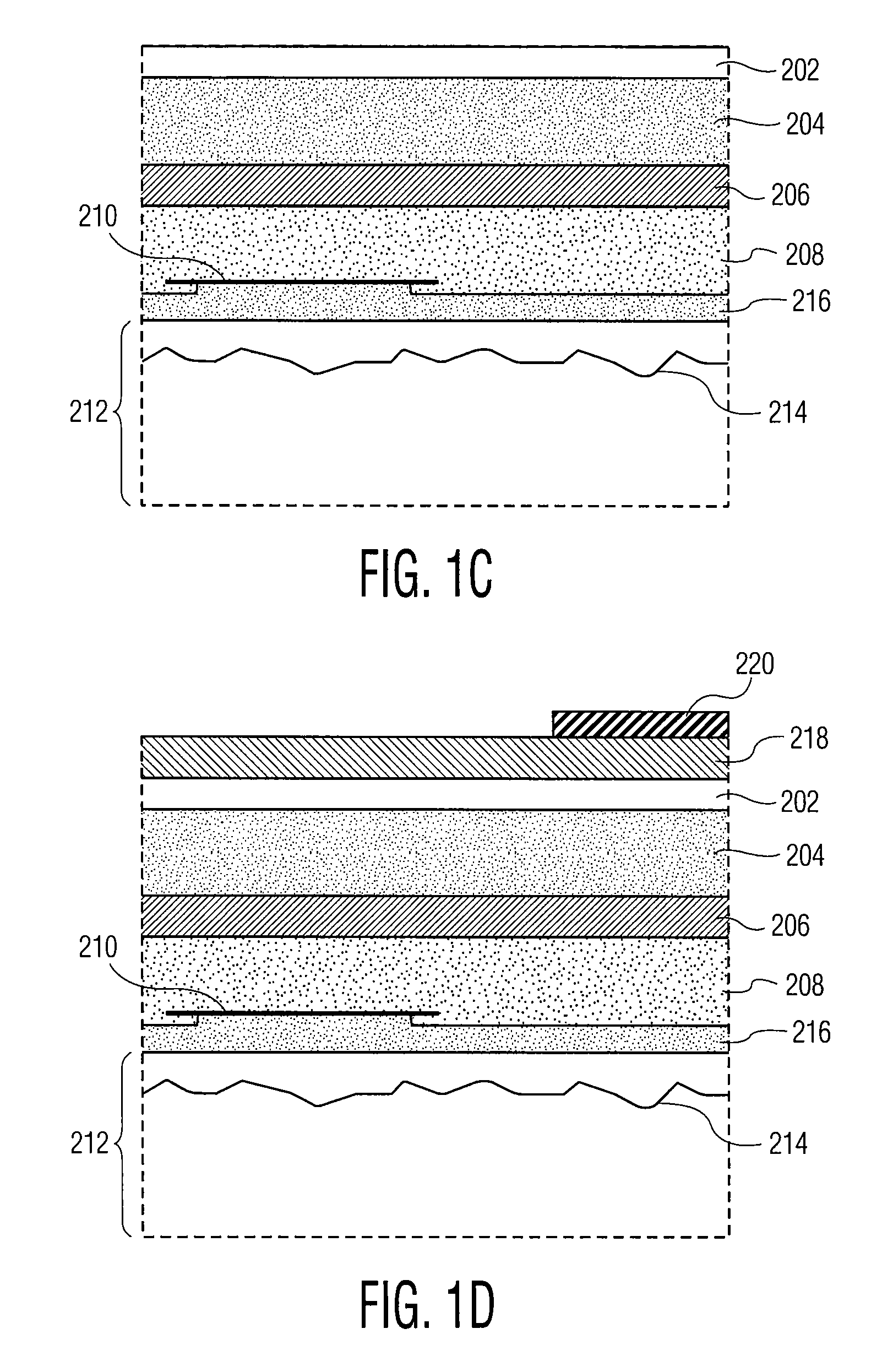
[0015]As described above, it may be necessary to thin the substrate of a backside illuminated imager to allow light to propagate through the substrate and to reach the photosensitive elements. For a silicon substrate, it may be desirable to thin the silicon to no more than a few microns, which is far below the minimum thickness required to provide mechanical integrity for wafer handling during processing. Accordingly, the embodiments of the present invention address construction methods for image sensors that provide mechanical integrity for wafer handling during processing and for high temperature processing to take place before color filters are placed.

[0016]FIGS. 1A-G and 2 illustrate steps in an example construction method for backside illuminated image sensors according to a first embodiment of the present invention. The first embodiment may include using a sacrificial handle wafer to provide mechanical stability for a semiconductor wafer during first processing steps and using...


PUM


Abstract

A method of constructing a backside illuminated image sensor is described. The method includes the steps of forming a semiconductor wafer, forming at least electrical contacts in the semiconductor wafer, forming, in a handle wafer separate from the semiconductor wafer, a plurality of via holes, attaching the semiconductor wafer to the handle wafer such that the via holes in the handle wafer are aligned with the respective electrical contacts on the semiconductor wafer, removing the substrate layer from the semiconductor wafer, removing at least a portion of the handle wafer to expose the plurality of via holes, filling each of the exposed via holes with a conductive material and applying a solder material to each of the exposed via holes such that the conductive material in each of the via holes is electrically connected to the solder material.

Description

BACKGROUND OF THE INVENTION[0001]The present invention relates to construction methods for backside illuminated image sensors and, more particularly, to construction methods for backside illuminated image sensors using improved methods for providing mechanical integrity for the semiconductor wafer during processing and performing high temperature processing out of the presence of color filters.[0002]Solid state image sensors, including complimentary metal oxide semiconductor (CMOS) imagers and charge-coupled devices (CCD), may be used in many different digital imaging applications to capture scenes. A solid state image sensor may include an array of pixels arranged on a semiconductor wafer. Pixel arrays may be formed on semiconductor wafers using semiconductor processing techniques such as, for example, photolithography, ion implantation, oxidation, thin film deposition and etching. When exposed to incident light to capture a scene, a photosensitive element of each pixel in the arra...

Claims


Application Information

Patent Timeline
Patent Type & Authority Applications(United States)
IPC IPC(8): H01L21/30H01L31/0232
CPCH01L21/76898H01L23/481H01L27/14687H01L2224/131H01L27/1464H01L2224/0401H01L2224/05H01L2224/11H01L2224/13H01L2224/13009H01L2924/014
Inventor DUNGAN, THOMAS EDWARDFARNWORTH, WARREN
Owner APTINA IMAGING CORP
Why Eureka
Try Eureka