Semiconductor package and semiconductor device

Inactive Publication Date: 2009-07-09
RENESAS TECH CORP
View PDF1 Cites 18 Cited by
  • Summary
  • Abstract
  • Description
  • Claims
  • Application Information

AI Technical Summary

Benefits of technology

[0020]According to the present invention, a semiconductor package which was tested beforehand and encapsulated can be operated by connecting with another semiconductor chips, such as dedicated system LSI which is functioning, combining the chip whose function is different, and systematization can be aimed at easily.
[0021]A companion failure that another semiconductor chips combined with this cannot be used in s

Problems solved by technology

Further, since electric inspection is conducted after assembly completion of a plurality of chips, there are many generation losses of a defective and a manufacture cost reduction is difficult.
Since a deg

Method used


Image

  • Semiconductor package and semiconductor device
  • Semiconductor package and semiconductor device
  • Semiconductor package and semiconductor device

Examples


Example

Example 1

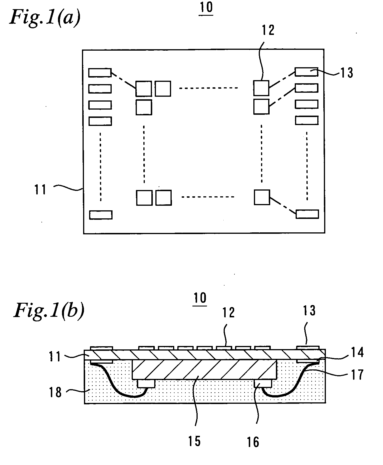
[0062]FIG. 1 is a drawing showing the structure of the encapsulated semiconductor package in Example 1 of this invention, the figure (a) shows a plan view and the figure (b) shows a sectional view.

[0063]In semiconductor package 10 of FIG. 1, on the surface of substrate 11 called an interposer or an interposer substrate, a plurality of terminals 12 for a test and a plurality of terminals 13 for external connection are arranged, and a plurality of terminals 14 for internal connection are arranged on the back surface. Internal connection of the terminal 14 for internal connection is made to desired terminal 12 for a test. Internal connection of the terminal 14 for internal connection is made also to desired terminal 13 for external connection. Although usually one terminal 12 for a test corresponds to one terminal 13 for external connection in the condition that electric connection is made mutually, there may be terminal 12 for a test without corresponding external connection ...

Example

Example 2

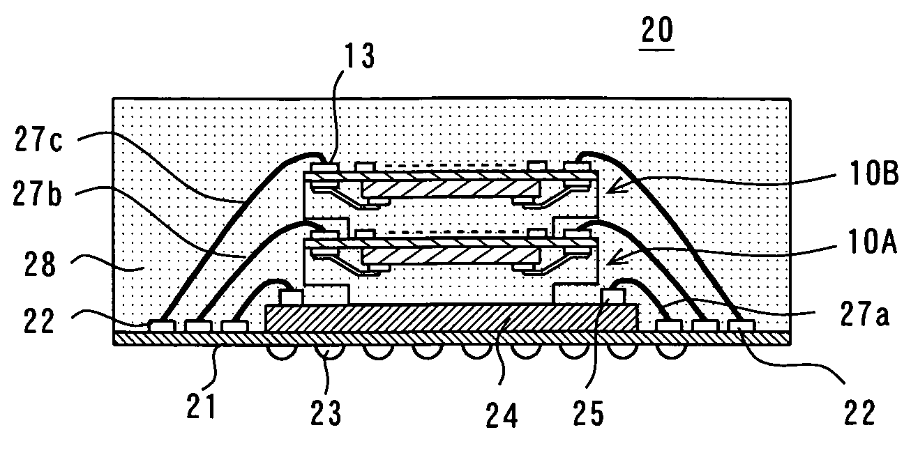
[0088]FIG. 2 is a sectional view showing the structure of semiconductor device 20 in Example 2 of this invention. In this semiconductor device 20, semiconductor package 10 which was explained in Example 1 and which was encapsulated is stacked in layers on a semiconductor chip, such as another integrated circuit device, and is made a package product of multichip.

[0089]In semiconductor device 20 shown in FIG. 2, a plurality of main terminals 22 for connection are arranged on the main front surface (upper part side of a sectional view) of main substrate 21 called an “interposer” or an “interposer substrate”, and a plurality of main terminals 23 for external connection are arranged on the back surface. And internal connection of the main terminal 22 for connection is made to desired main terminal 23 for external connection.

[0090]A main semiconductor chip 24 is arranged on the front surface of main substrate 21, facing the back surface (lower part side of a sectional view) to it...

Example

Example 3

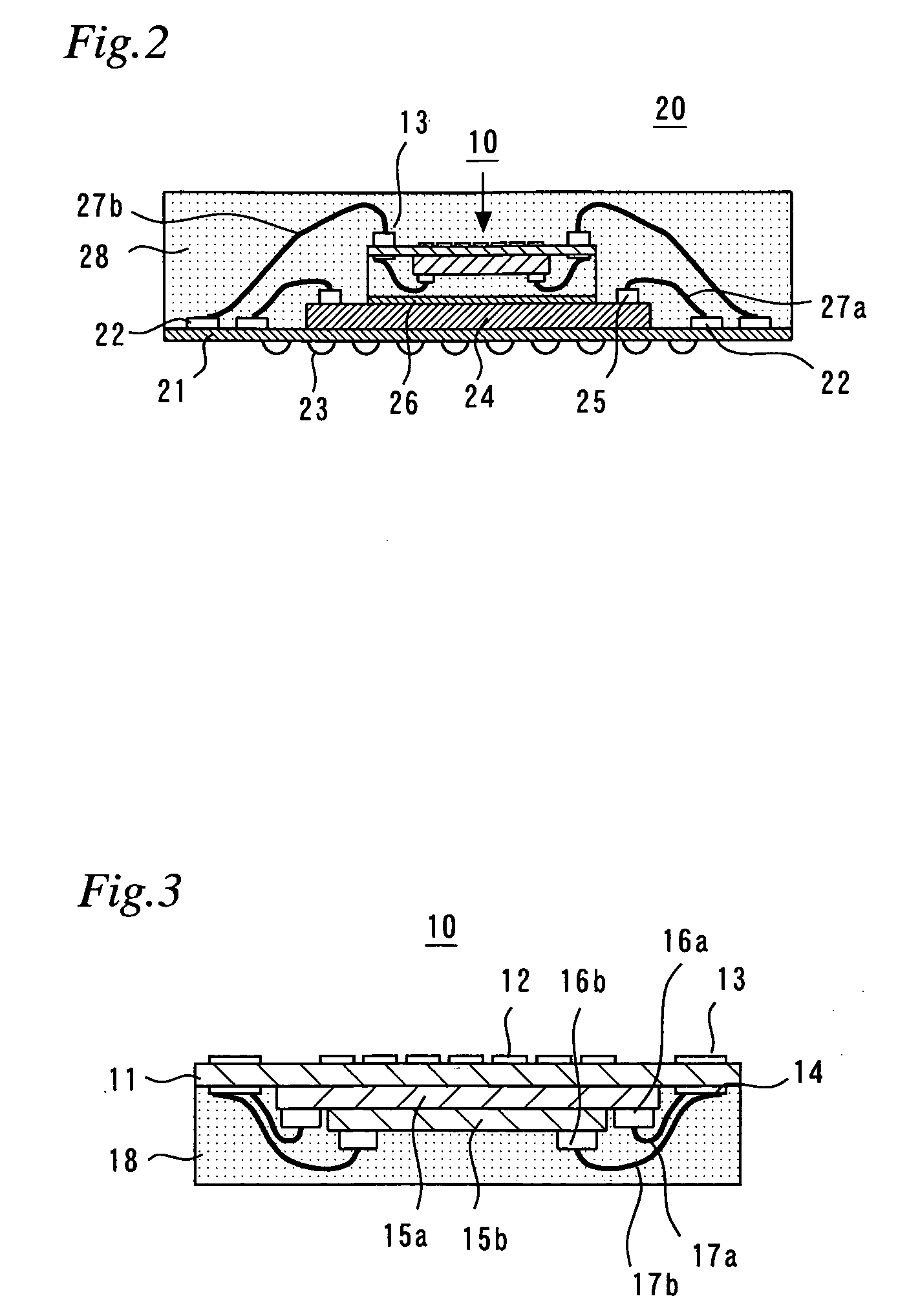
[0106]FIG. 3 is a sectional view showing the structure of the semiconductor package by another examples of this invention.

[0107]In this example, two semiconductor chips 15a and 15b are arranged on the back surface of substrate 11, and surface terminals 16a and 16b which are arranged on the front surface of semiconductor chips 15a and 15b are connected to terminal 14 for internal connection of the back surface of substrate 11, respectively.

[0108]Seeing from the substrate 11 side, surface terminal 16a is arranged at the periphery of the front surface of semiconductor chip 15a of the lower berth, and semiconductor chip 15b of the upper berth is arranged on the non-terminal area of the inside. The semiconductor chips to be stacked in layers are not restricted to two pieces, but those of two or more required number can be stacked in layers. Substrate 11 and semiconductor chips 15a and 15b may be adhered by an adhesive layer. An integration degree can be raised by such stacked la...


PUM


Abstract

A package structure which aims at improvement in function, miniaturization, and systematization of a semiconductor integrated circuit having been made into multichip is offered.
A substrate in which a plurality of terminals for a test and a plurality of terminals for external connection are arranged on the front surface, and a plurality of terminals for internal connection are arranged on the back surface, and a semiconductor chip in which a plurality of surface terminals connected to an internal circuit are formed in the front surface are prepared. An encapsulated semiconductor package is formed by joining the back surface of this semiconductor chip to the back surface of the substrate, connecting the surface terminal of the semiconductor chip to the desired terminal for internal connection of the substrate, and sealing the semiconductor chip on the back surface of the substrate with a molded member. A multichip structure is made by joining the encapsulated semiconductor package to another semiconductor chip mounted on the substrate formed external connection terminals and sealing them.

Description

INCORPORATION BY REFERENCE[0001]The present application claims priority from PCT application PCT / JP2005 / 000235 filed on Jan. 12, 2005, the content of which is hereby incorporated by reference into this application.TECHNICAL FIELD[0002]The present invention relates to an encapsulated semiconductor package and a semiconductor device incorporating this semiconductor package.BACKGROUND ART[0003]Regarding functional improvement, miniaturization, and systematization of a semiconductor device used now, a multichip package which accumulates a plurality of IC chips directly and perpendicularly, and makes wire bonding to an interposer board directly is used centering on a memory kind. (For example, refer to Patent Reference 1, 2).[0004][Patent Reference 1] Japanese Unexamined Patent Publication No. 2002-231885[0005][Patent Reference 2] Japanese Unexamined Patent Publication No. 2002-217367DISCLOSURE OF THE INVENTION[0006]Since a chip mounting surface is single, generally versatility of a comb...

Claims


Application Information

Patent Timeline
IPC IPC(8): H01L25/04H01L25/18H01L23/12H01L23/31H01L23/433H01L23/48H01L25/10H01L25/11
CPCH01L23/3121H01L23/3135H01L23/4334H01L25/03H01L2224/48225H01L2224/48227H01L24/48H01L2924/15311H01L2224/32145H01L2224/32225H01L2224/73265H01L2924/1815H01L2924/19107H01L2224/73215H01L2924/00012H01L2924/00H01L24/73H01L2924/14H01L2924/181H01L2224/4917H01L2924/00014H01L24/49H01L2224/45099H01L2224/45015H01L2924/207H01L23/48H01L23/12
Inventor OSAKA, SHUICHIFUJIMOTO, HITOSHIHIROSE, TETSUYASHINONAGA, NAOYUKI
Owner RENESAS TECH CORP
Why Eureka
Try Eureka