
Non-volatile semiconductor memory device and memory system including the same

a non-volatile semiconductor and memory cell technology, applied in static storage, digital storage, instruments, etc., can solve the problems of lowering the voltage applied to the drain of the memory cell, the difficulty of making the inability to make a reading speed fast, etc., and achieve the effect of variable sector capacity

Active Publication Date: 2009-07-16
SAMSUNG ELECTRONICS CO LTD
View PDF11 Cites 6 Cited by
  • Summary
  • Abstract
  • Description
  • Claims
  • Application Information

AI Technical Summary

Benefits of technology

[0015]The present invention provides a non-volatile semiconductor memory device having various advantages. They are as follows. A time for receiving drain disturb is the same as before. It is useful in terms of a layout. A sector capacity is variable while maintaining a chip capacity.

Problems solved by technology

However, if the above methods are used, there are several difficulties as follows.
Therefore, it is difficult to make a reading speed fast and thus it may become slower.
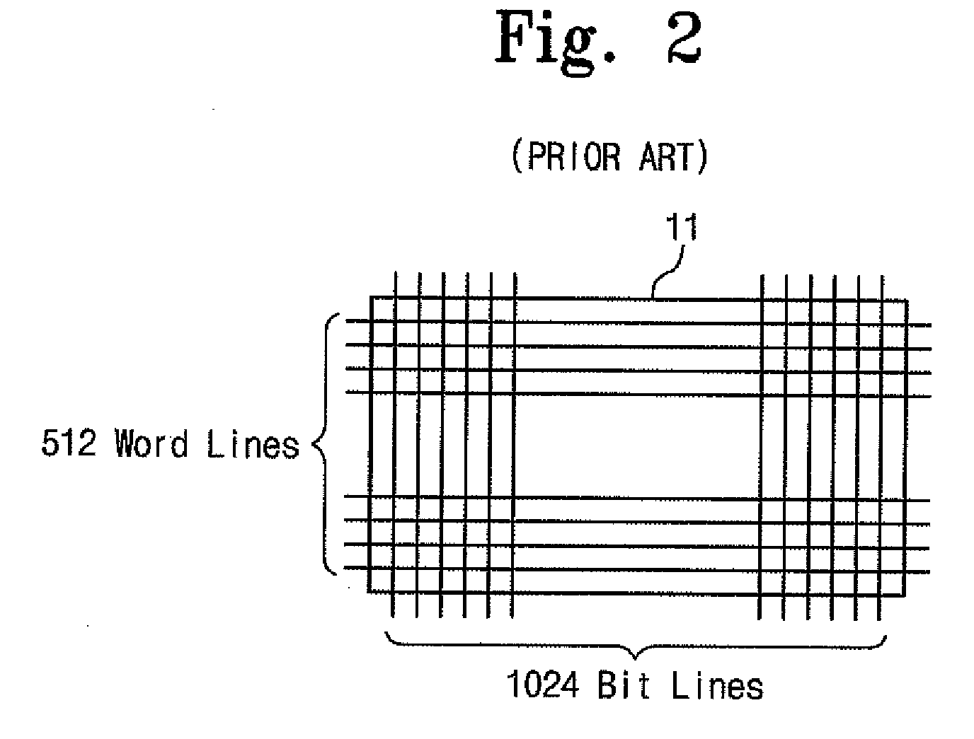
Additionally, during an input operation of a memory cell, because of a bit line resistance, an actual voltage applied to a drain of a memory cell is lowered, and input characteristics in a sector are deteriorated.
Accordingly, when considering a cycling characteristics of a sector, drain disturb in a memory cell becomes four times typical drain disturb, and thus, it may be hard to obtain reliability.
However, in an aspect of cycling, drain disturb still remains.
Therefore, this situation is unfavorable.

Method used


Image

  • Non-volatile semiconductor memory device and memory system including the same
  • Non-volatile semiconductor memory device and memory system including the same
  • Non-volatile semiconductor memory device and memory system including the same

Examples


Embodiment Construction

[0036]Preferred embodiments of the present invention will be described below in more detail with reference to the accompanying drawings. The present invention may, however, be embodied in different forms and should not be construed as limited to the embodiments set forth herein. Rather, these embodiments are provided so that this disclosure will be thorough and complete, and will fully convey the scope of the present invention to those skilled in the art.

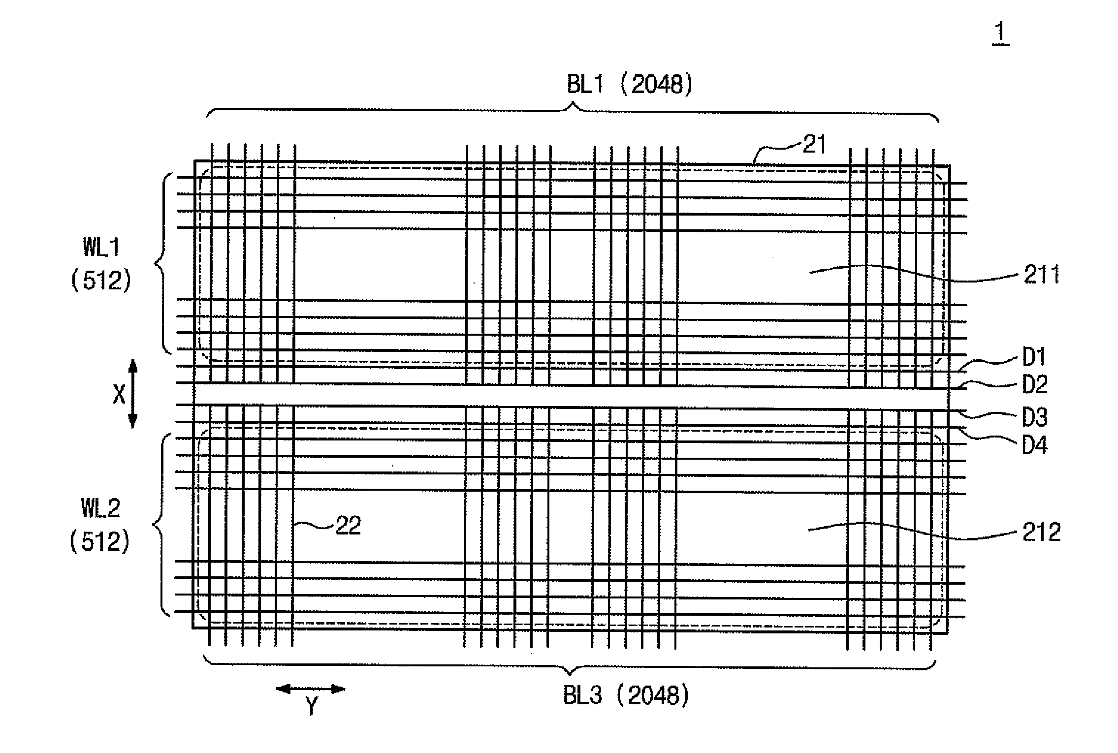
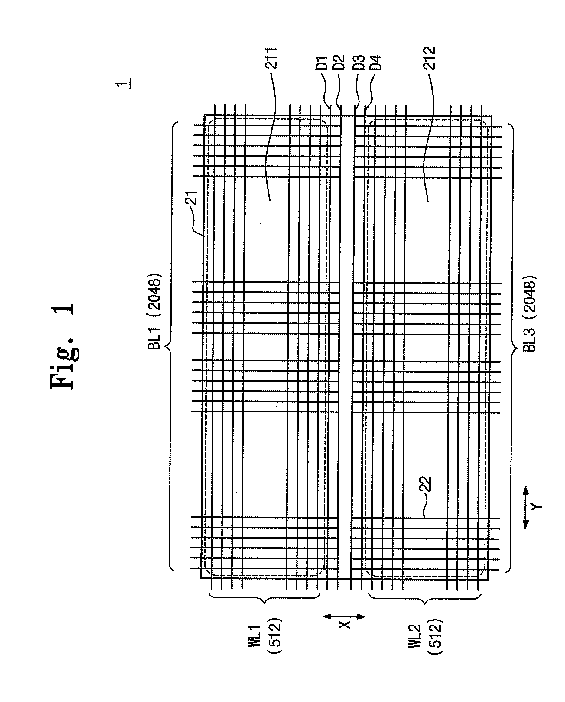
[0037]FIG. 1 is used for describing a non-volatile semiconductor memory device according to an embodiment of the present invention and is a plan view illustrating a memory cell array structure of a flash memory. In FIG. 1, a reference number 21 refers to one rectangular P-well region for forming a memory cell array. Reference symbols D1 to D4 refer to a plurality (i.e., four) of dummy word lines. A reference symbol WL1 refers to a first word line group. A reference symbol WL2 refers to a second word line group. A reference number 22...


PUM


Abstract

Provided is a non-volatile semiconductor device. The non-volatile semiconductor memory devices including: first and second word line groups disposed in parallel; dummy word lines disposed between the first and second word line groups; a first bit line group intersecting the first word line group; and a second bit line group intersecting the second word line group, wherein the first and second word line groups, the first and second bit line groups, and the dummy word lines are disposed on a same well.

Description

CROSS-REFERENCE TO RELATED APPLICATIONS[0001]This U.S. non-provisional patent application claims priority under 35 U.S.C. § 119 of Japanese Patent Application No. 2007-332365, filed on Dec. 25, 2007 and Korea Patent Application No. 2008-127432 filed on Dec. 15, 2008, the entire contents of which are hereby incorporated by reference.BACKGROUND OF THE INVENTION[0002]The present invention disclosed herein relates to a non-volatile semiconductor device, and more particularly, to a memory cell array of a flash memory.[0003]Recently, demands for increasing a capacity of an erase sector (hereinafter, referred to as a sector) have been increased. Although typical sector capacity is 0.5 Mbits, products having a sector capacity of 2 Mbits are developed and extensively used. This is because a multi-level cell (MLC) is applied to a semiconductor device and its chip size is miniaturized.[0004]If a memory having the same capacity as the MLC is realized with a single-level cell (SLC) technique, th...

Claims


Application Information

Patent Timeline
Patent Type & Authority Applications(United States)
IPC IPC(8): G11C16/04G11C5/02G11C16/06
CPCG11C16/16G11C8/14
Inventor KAWAMURA, SHOICHI
Owner SAMSUNG ELECTRONICS CO LTD
Learn More