Sensor, solid-state imaging device, and imaging apparatus and method of manufacturing the same

a solid-state imaging and sensor technology, applied in the direction of solid-state devices, transistors, spectral investigation, etc., can solve the problems of extreme decrease in sensitivity, decrease in light received, and decrease in sensitivity to light at a shorter wavelength region, so as to achieve high-sensitivity determination of spectroscopic characteristics

Inactive Publication Date: 2009-07-23
SONY CORP
View PDF2 Cites 21 Cited by
  • Summary
  • Abstract
  • Description
  • Claims
  • Application Information

AI Technical Summary

Benefits of technology

[0018]According to the above embodiments of the invention, the use of the single photodiode allows a high sensitive determination of the spectroscopic characteristics.

Problems solved by technology

Thus, an opening area for the incident light may be narrow, causing a decrease in amount of light received.
Furthermore, it also results in a decrease in sensitivity.
In addition, the use of a transparent electrode leads to an extreme decrease in sensitivity to light at a shorter wavelength region, such as ultraviolet or blue region.

Method used


Image

  • Sensor, solid-state imaging device, and imaging apparatus and method of manufacturing the same
  • Sensor, solid-state imaging device, and imaging apparatus and method of manufacturing the same
  • Sensor, solid-state imaging device, and imaging apparatus and method of manufacturing the same

Examples


Embodiment Construction

[0032]Prior to describing specific examples according to an embodiment of the present invention, the outline of the present invention will be described.

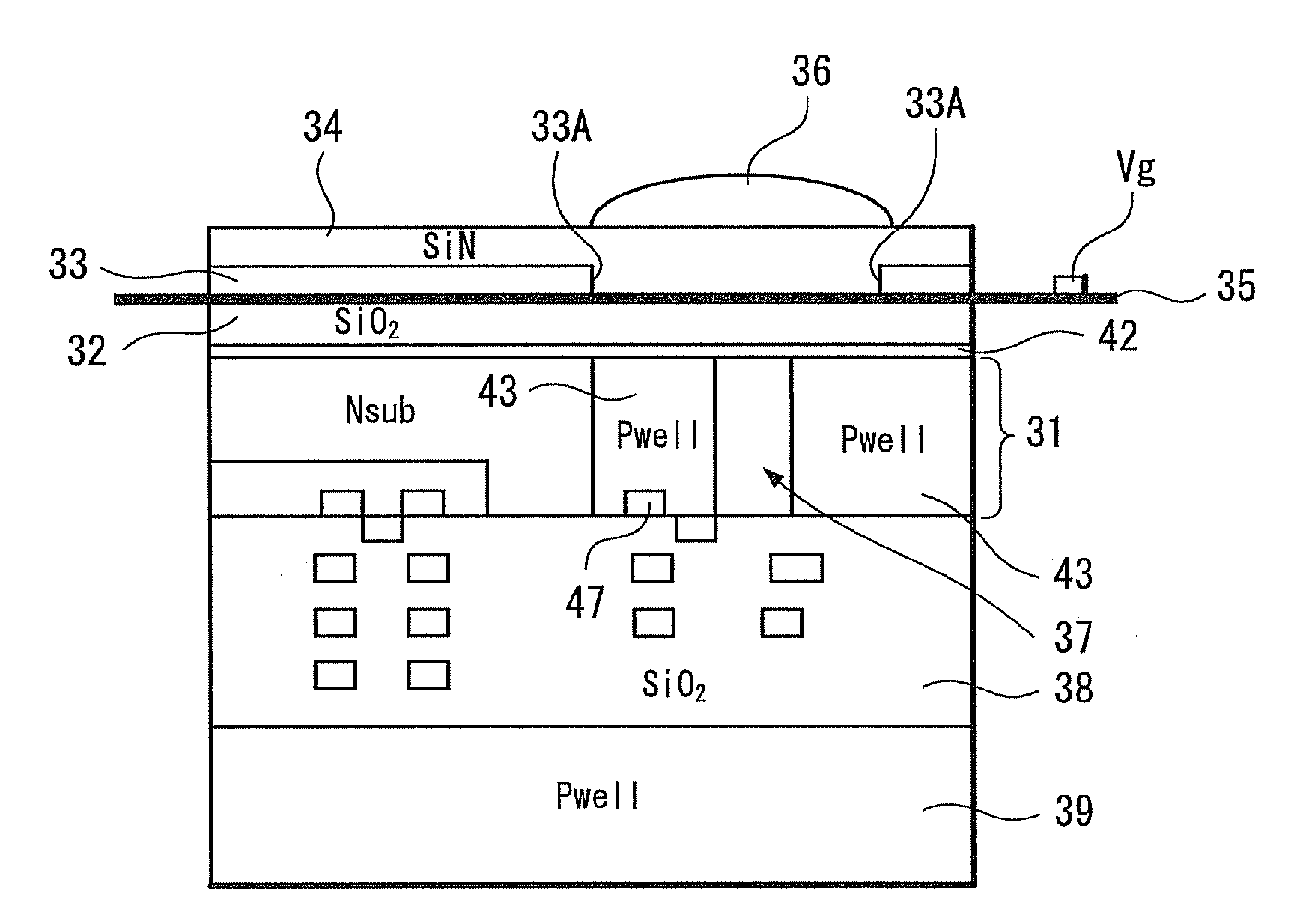
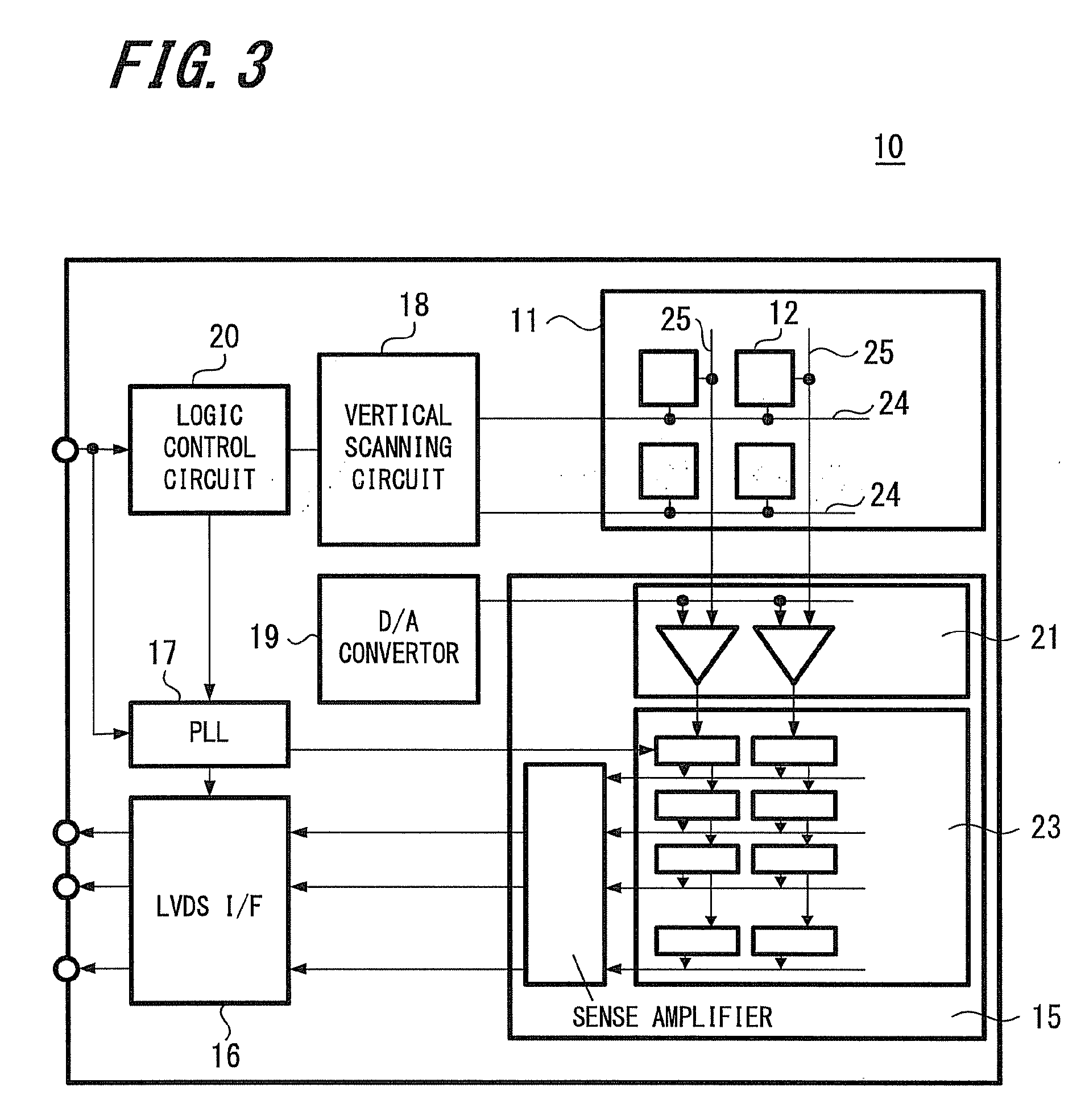
[0033]According to an embodiment of the present invention, there is provided an imaging device which can carry out spectroscopic measurement. Light incident on the semiconductor device enters the semiconductor device and the wavelength of light to be subjected to photoelectric conversion varies depending on the depth from the surface of the device. Using such characteristics of the light, a gate electrode is mounted on a sensor in the semiconductor device to carry out variable control of the potential of a quantum well structure in which electrons converted from photons are accumulated, allowing the measurement of spectral characteristics. Furthermore, a solid-state imaging device for obtaining a color image from the measured spectral characteristics can be configured using such a sensor as a pixel.

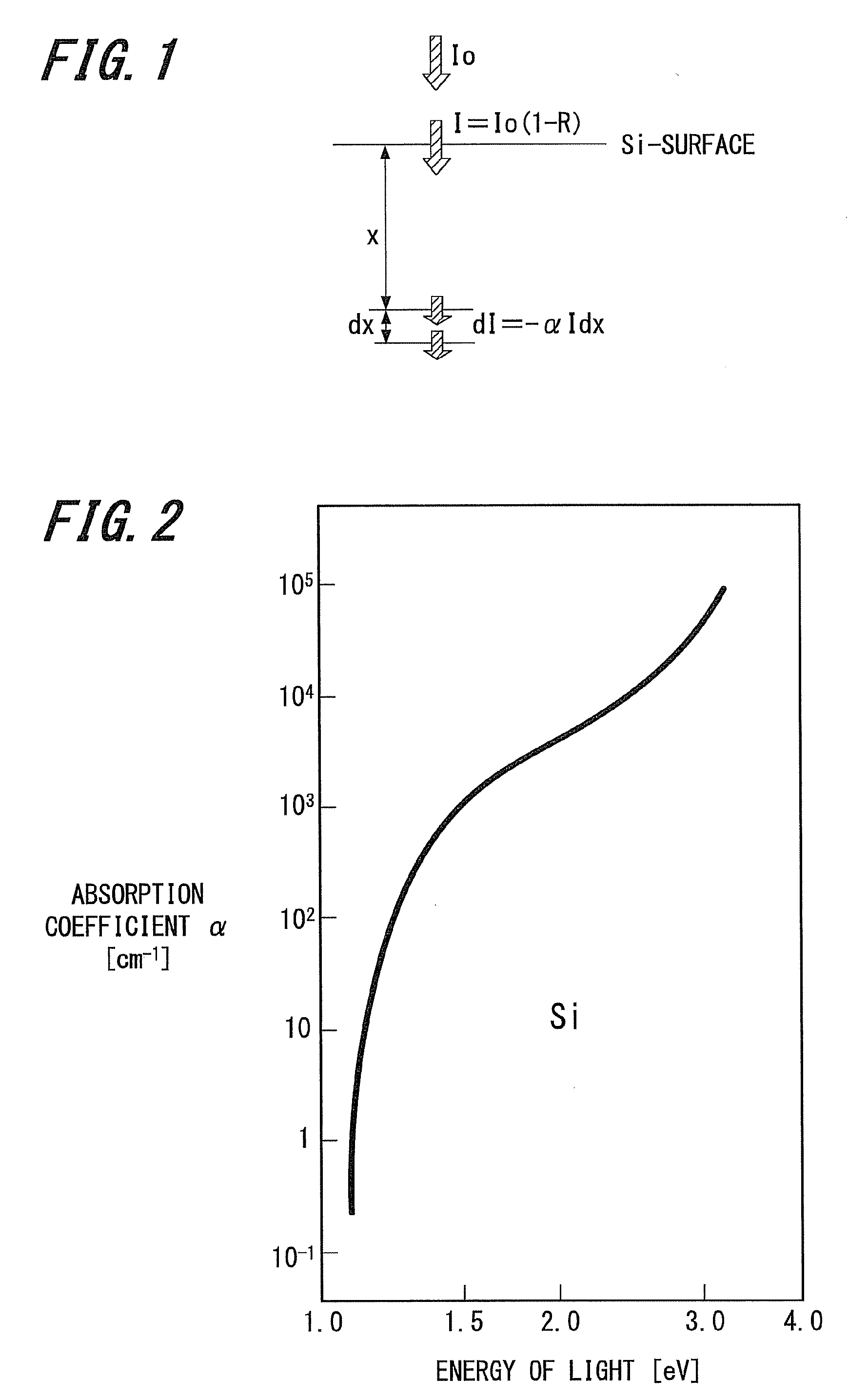
[0034]First, the basic principle fo...


PUM


Abstract

A sensor is provided. The sensor includes semiconductor layer; a photodiode, an impurity-doped polycrystalline silicon layer; and a gate electrode. The photodiode is formed in the semiconductor layer. The impurity-doped polycrystalline silicon layer is formed above the semiconductor layer. The gate electrode applies a gate voltage to the polycrystalline silicon layer. A wiring layer is provided on a first surface of the semiconductor layer and light is incident on a second surface thereof.

Description

CROSS REFERENCES TO RELATED APPLICATIONS[0001]The present invention contains subject matter related to Japanese Patent Application JP 2008-009474 filed in the Japanese Patent Office on Jan. 18, 2008, the entire contents of which being incorporated herein by reference.BACKGROUND OF THE INVENTION[0002]1. Field of the Invention[0003]The present invention relates to a sensor for detecting the wavelength and intensity of incident light. The present invention also relates to a solid-state imaging device. The present invention further relates to an imaging apparatus using such a solid-state imaging device and a method of manufacturing the same.[0004]2. Description of the Related Art[0005]An attempt for obtaining information about three primary colors (RGB) by a single photodiode has been conducted (see, for example, U.S. Pat. No. 5,965,875).[0006]The photodiode as described in U.S. Pat. No. 5,965,875 has an arrangement of pixels where each pixel includes a stacked structure of three diffus...

Claims


Application Information

Patent Timeline
Patent Type & Authority Applications(United States)
IPC IPC(8): H01L31/02H01L31/0368H01L29/788
CPCH01L27/14609H01L27/14627H01L27/1464H01L27/14687H01L27/14643G01J3/30H01L31/10
Inventor TAKEUCHI, KIYOSHI
Owner SONY CORP
Why Eureka
Try Eureka