

Organic el device
a technology of organic el and electrodes, applied in the direction of organic semiconductor devices, discharge tubes/lamp details, discharge tubes luminescent screens, etc., can solve the problems of disconnection between the electrode and the conductive member, insufficient electrode coverage,
- Summary
- Abstract
- Description
- Claims
- Application Information
AI Technical Summary
Benefits of technology
Problems solved by technology
Method used
Image

Examples
first embodiment
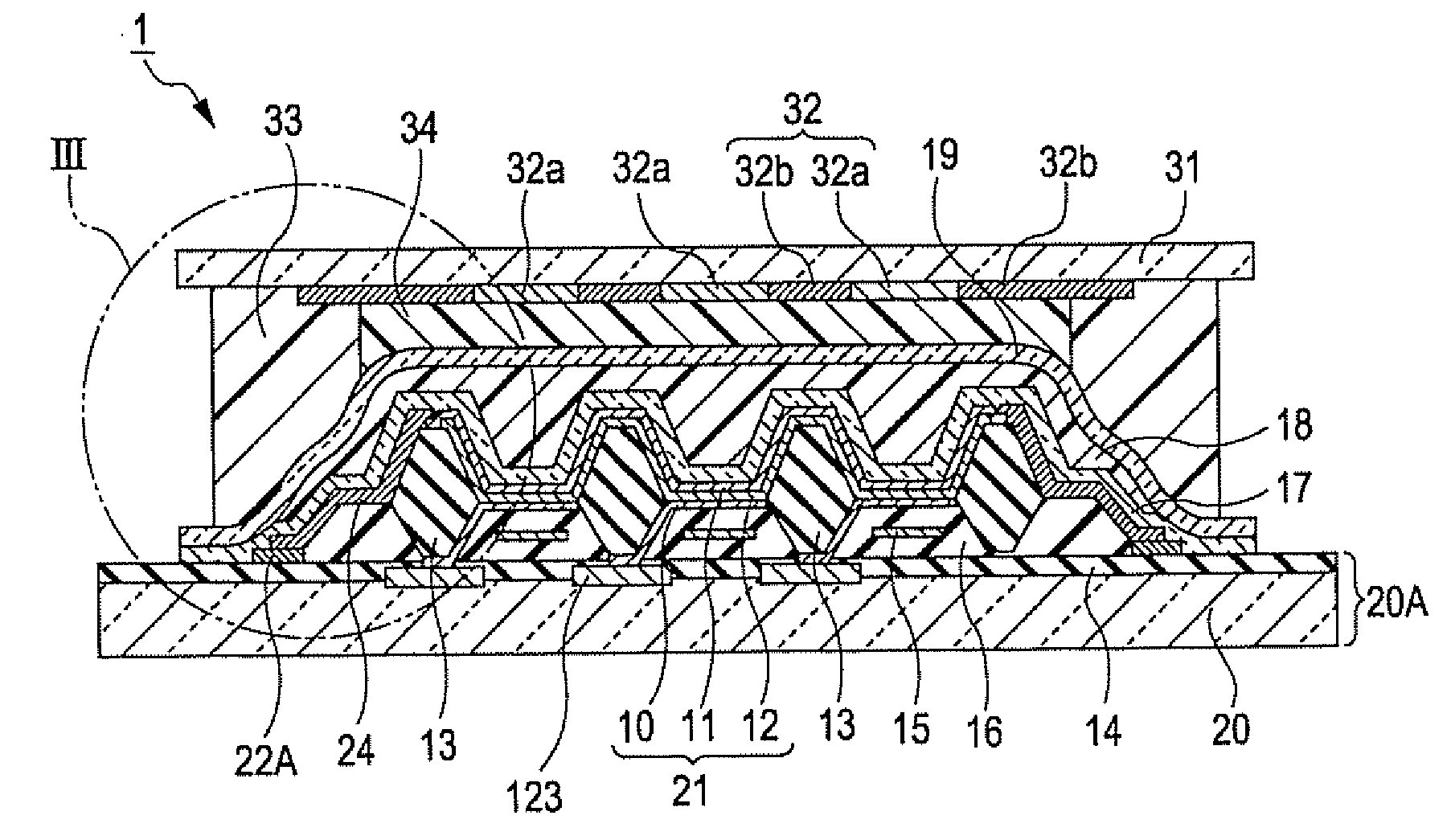
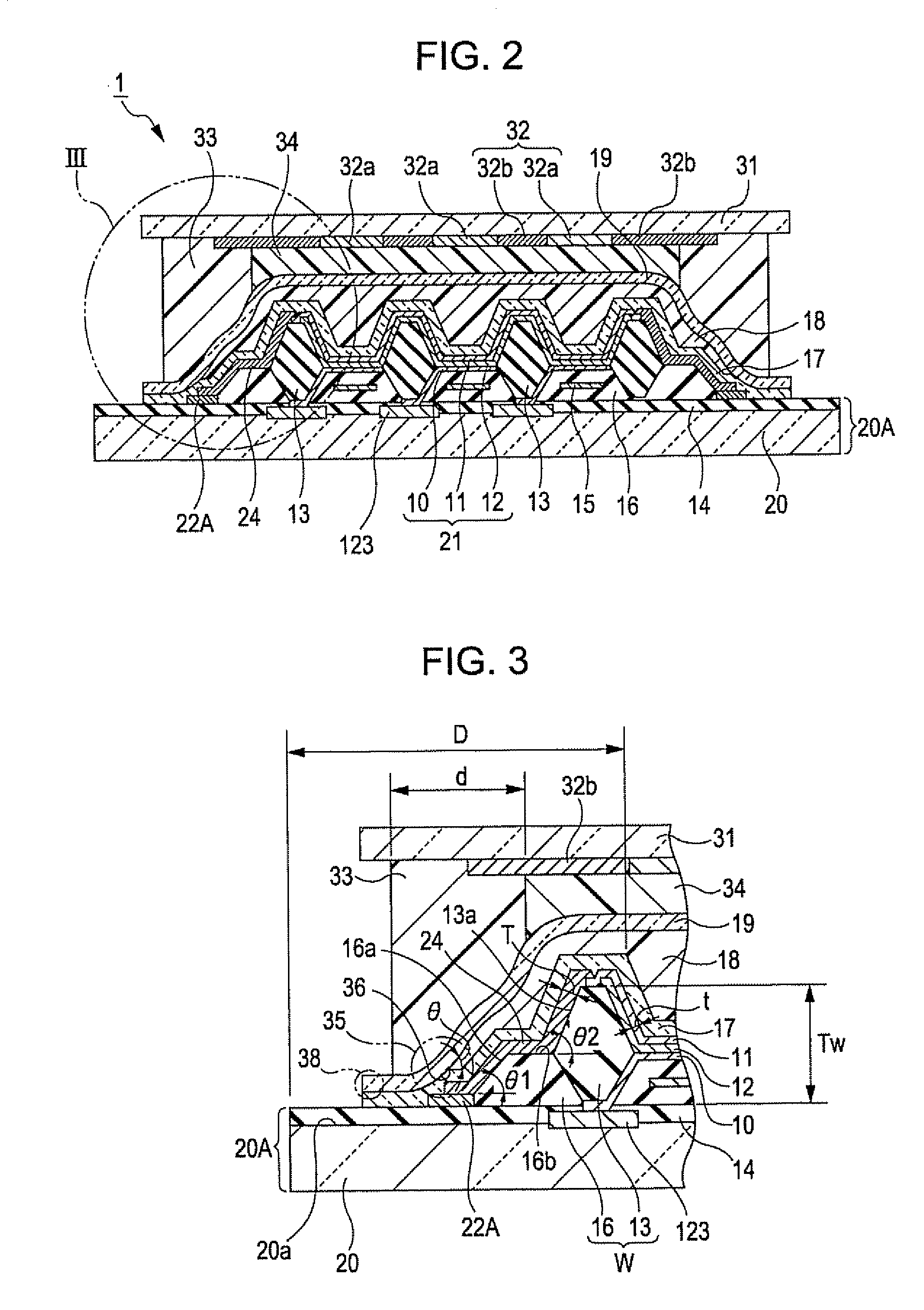
[0034]A first embodiment of the invention will be described with reference to the drawings. In the drawings, in order to make the individual layers and components recognizable, different scales are used for the individual layers and components.
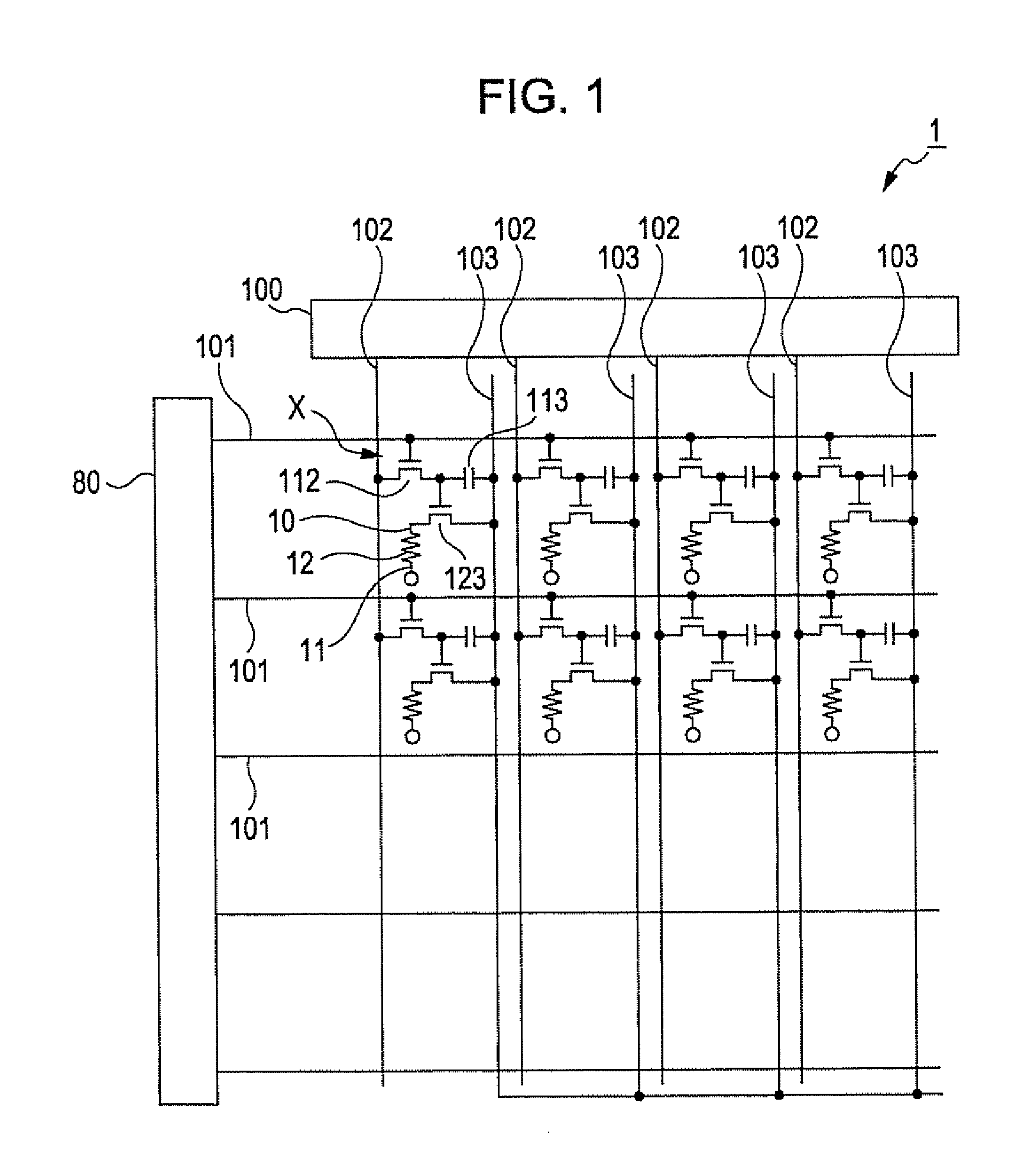
[0035]FIG. 1 is a schematic diagram showing a wiring structure of an organic EL device according to the first embodiment. An organic EL device 1 is an active matrix-type device in which thin-film transistors (hereinafter referred to as “TFTs”) are used as switching elements. The organic EL device 1 has a wiring structure in which a plurality of scanning lines 101, a plurality of signal lines 102 extending in a direction orthogonal to the scanning lines 101, and a plurality of power lines 103 extending parallel to the signal lines 102 are arranged. A sub-pixel X is disposed in the vicinity of each of the intersections of the scanning lines 101 and the signal lines 102.
[0036]The signal lines 102 are connected to a data line driving circuit 100 h...
second embodiment
[0112]A second embodiment of the invention will be described with reference to FIGS. 1 to 3 and newly to FIG. 5. An organic EL device according to the second embodiment differs from the organic EL device 1 described in the first embodiment in that a cathode connection layer 24B is disposed continuously along three sides of the enclosing member W. Otherwise, the second embodiment is the same as the first embodiment. Consequently, the same components or parts as those of the first embodiment are designated by the same reference numerals, and description thereof is omitted.
[0113]As shown in FIG. 5, in an organic EL device 1B according to this embodiment, the cathode connection layer 24B extends like a strip along three sides of the enclosing member W. Thereby, the connection area between each of the cathode 11 of the light emitting elements 21 and the first cathode line 22A and the cathode connection layer 24B can be increased, resulting in a decrease in connection resistance, and the ...
PUM
 Abstract
Description
Claims
Application Information