Semiconductor device

a semiconductor device and on-resistance technology, applied in the direction of semiconductor devices, electrical equipment, transistors, etc., can solve the problems of hindering the reduction of on-resistance in the semiconductor device, reducing connection-resistance, and high drain region resistance

Inactive Publication Date: 2006-06-08
SANYO ELECTRIC CO LTD
View PDF18 Cites 16 Cited by
  • Summary
  • Abstract
  • Description
  • Claims
  • Application Information

AI Technical Summary

Benefits of technology

[0018] However, a current flows from one of the MOSFETs to the other by passing through the drain region 132 and the substrate 131. In other words, the current path has a long route, and thus resistance in the drain region becomes high. Flip-chip mounting as shown in FIGS. 5C and 5D is what can at least reduce connection-resistance with external terminals as compared with mounting according to a wire-bonding method. The wire-bonding method is a method whereby a back surface of a chip is bonded to a lead frame, and the lead frame forming an external terminal is connected to a source electrode and a gate pad electrode by use of a bonding wire. However, the flip-chip mounting is affected by the resistance in the substrate, and thereby has a problem that reduction in on-resistance in a semiconductor device is hindered.

Problems solved by technology

However, the flip-chip mounting is affected by the resistance in the substrate, and thereby has a problem that reduction in on-resistance in a semiconductor device is hindered.

Method used


Image

  • Semiconductor device
  • Semiconductor device
  • Semiconductor device

Examples


Embodiment Construction

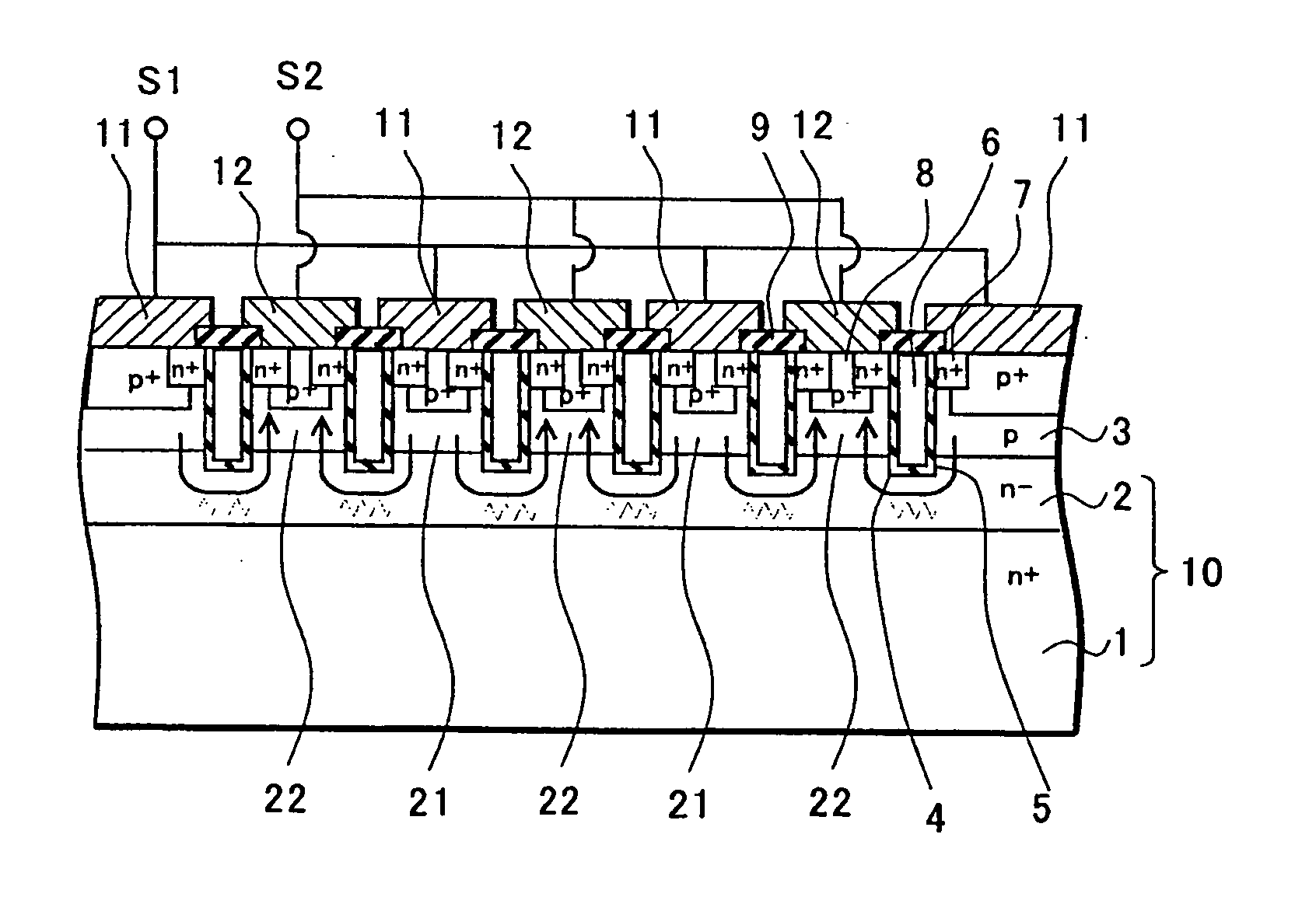
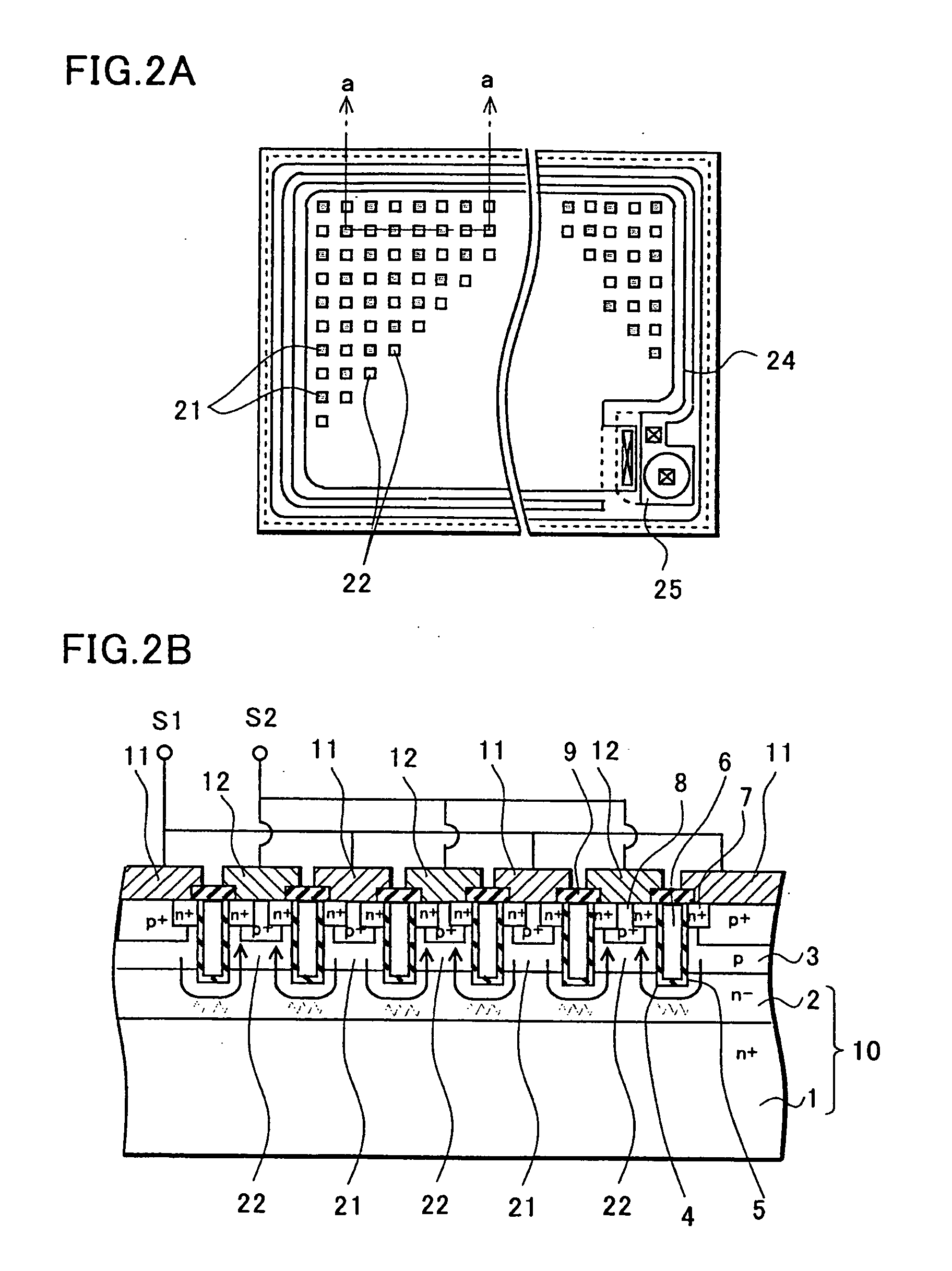
[0028] With reference to FIGS. 1 to 4, a detailed description will be given of an embodiment of the present invention by taking an n-channel MOSFET as an example.

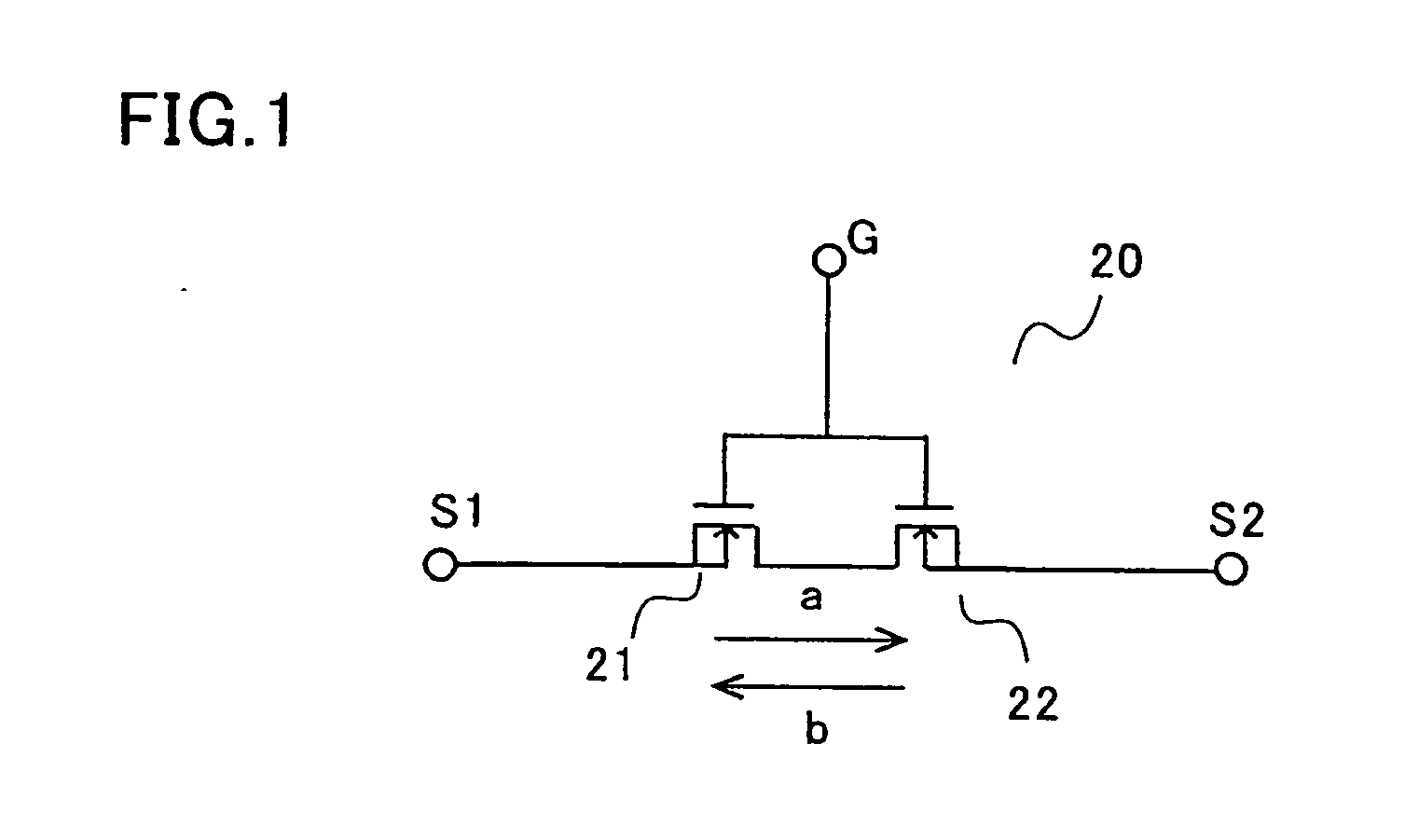
[0029]FIG. 1 is a schematic circuit diagram explaining a semiconductor device 20 according to the embodiment.

[0030] The semiconductor device 20 according to the embodiment is a MOSFET in which a plurality of MOS transistors 21 and a plurality of MOS transistors 22 are arranged on a substrate forming a drain region. The MOSFET 20 is connected to a gate terminal G and is controlled by a control signal applied to the gate terminal G. The gate terminal is only one.

[0031] The MOS transistors 21 and 22 are integrated on one chip, and terminals to be lead out externally are the gate terminal, a first and second source terminals S1 and S2. The drains for the MOS transistors 21 and 22 are common and connected to one another, whereby they are not lead out externally as drain terminals.

[0032] Different potentials are applied to th...


PUM


Abstract

In a preferred embodiment of the present invention, first MOS transistors connected to first source electrodes and second MOS transistors connected to second source electrodes are arranged alternately next to each other on one chip. Different potentials are applied respectively to the first source electrodes and to the second source electrodes, and both of the MOS transistors are controlled with respect to an ON or OFF state by one gate terminal. Currents flow along surroundings of trenches, whereby on-resistance is reduced.

Description

BACKGROUND OF THE INVENTION [0001] 1. Field of the Invention [0002] The present invention relates to a semiconductor device, and particularly to a semiconductor device realizing miniaturization of a switching element and reduction in on-resistance thereof, which is capable of switching a current path in two directions. [0003] 2. Description of the Related Art [0004] As a switching element, a switching element which not only switches a device between ON and OFF but also switches the direction of a current path (the direction in which a current flows) is also under development, and such a switching element is adopted, for example, to a protection circuit of a secondary battery. [0005]FIGS. 5A to 5D show an example of a switching element which switches a current path in two directions. [0006]FIG. 5A is a circuit diagram of the switching element. In a two-way switching element 30, first and second MOSFETs 31 and 32 are connected in series. Then, gate signals are respectively applied to ...

Claims


Application Information

Patent Timeline
Patent Type & Authority Applications(United States)
IPC IPC(8): H01L29/76
CPCH01L27/0266H01L29/0696H01L29/41758H01L2224/16245H01L2924/13091H01L29/7825H01L2924/00H01L2224/05573H01L2224/05568H01L2924/00014H01L2224/0554H01L2224/0603H01L2224/05599H01L2224/0555H01L2224/0556
Inventor YANAGIDA, MASAMICHIMANDAI, TADAO
Owner SANYO ELECTRIC CO LTD
Why Eureka
Try Eureka