Organic electroluminescent device and electronic apparatus

a technology of electroluminescent devices and electronic devices, which is applied in the direction of discharge tubes/lamp details, discharge tubes luminescnet screens, electric discharge lamps, etc., can solve the problems of large electrical resistance of second electrode layers, liable to generate the variations of luminescent light, and the above-mentioned problems, etc., to achieve high electric resistance, small area, and wide area

Active Publication Date: 2009-10-22
SEIKO EPSON CORP
View PDF8 Cites 15 Cited by
  • Summary
  • Abstract
  • Description
  • Claims
  • Application Information

AI Technical Summary

Benefits of technology

[0076]As described above, in this embodiment, since a plurality of the auxiliary wires 8a connected to the second electrode layer 9a extends in one direction at the lower layer side of the second electrode layer 9a which is formed to cover a plurality of the pixels 100a, a high electric resistance of the second electrode layer 9a can be compensated for by the auxiliary wires 8a, and in addition, local variation in electric resistance of the second electrode layer 9a can also be absorbed by the auxiliary wires 8a. Hence, luminance variation of the organic EL device 100 can be resolved.
[0077]In addition, in this embodiment, since the lower layer-side conductive pattern portion 6s for applying a potential to the second electrode layer 9a is formed at the lower layer side of the insulating film 115, and at the upper layer side of the insulating film 115, the upper layer-side conductive pattern portion 7s for connecting the second electrode layer 9a to the lower layer-side conductive pattern portion 6s is formed using a conductive film having a sheet resistance lower than that of the second electrode layer 9a, a potential can be applied from the terminal 104 to the auxiliary wires 8a and the second electrode layer 9a through the lower layer-side conductive pattern portion 6s and the upper layer-side conductive pattern portion 7s. In this embodiment, since the upper layer-side conductive pattern portion 7s has the contact pattern portion 7p provided on the upper surface of the lower layer-side conductive pattern portion 6s at the contact portion 115s, even when the contact portion 115s is narrow, the connection resistance between the lower layer-side conductive pattern portion 6s and the upper layer-side conductive pattern portion 7s is low.
[0078]In addition, since the upper layer-side conductive pattern portion 7s is formed on the insulating film 115, the upper layer-side conductive pattern portion 7s can also be electrically connected to the auxiliary wires 8a outside the contact portion 115s, and hence the structure in which the upper layer-side conductive pattern portion 7s and the auxiliary wires 8a are in contact with each other in a sufficiently wide area can be realized. Accordingly, without excessively increasing the area of the contact portion 115s, the second electrode layer 9a can be reliably connected to the lower layer-side conductive pattern portion 6s through the auxiliary wires 8a; hence, the peripheral region 110c, which is located outside the pixel region

Problems solved by technology

Among the organic EL devices as described above, in particular, in a top emission-type organic EL device in which light emitted from an organic EL element is emitted through a second electrode layer, since the second electrode layer is required to have light transparency, the thickness thereof is small, and as a result, luminescent variation caused by electrical resista

Method used


Image

  • Organic electroluminescent device and electronic apparatus
  • Organic electroluminescent device and electronic apparatus
  • Organic electroluminescent device and electronic apparatus

Examples


embodiment 1

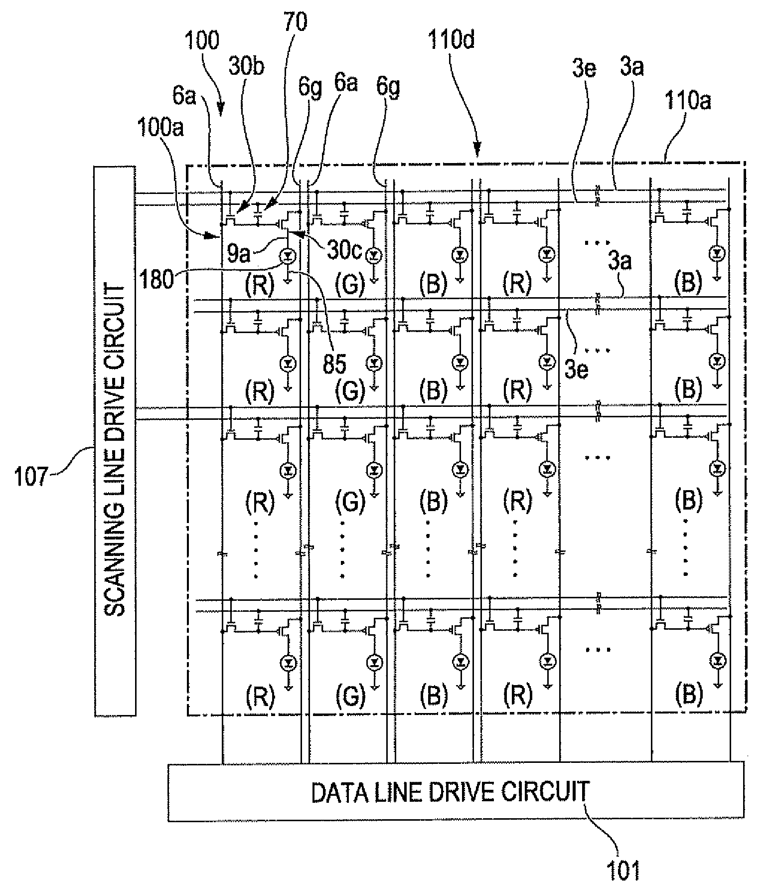
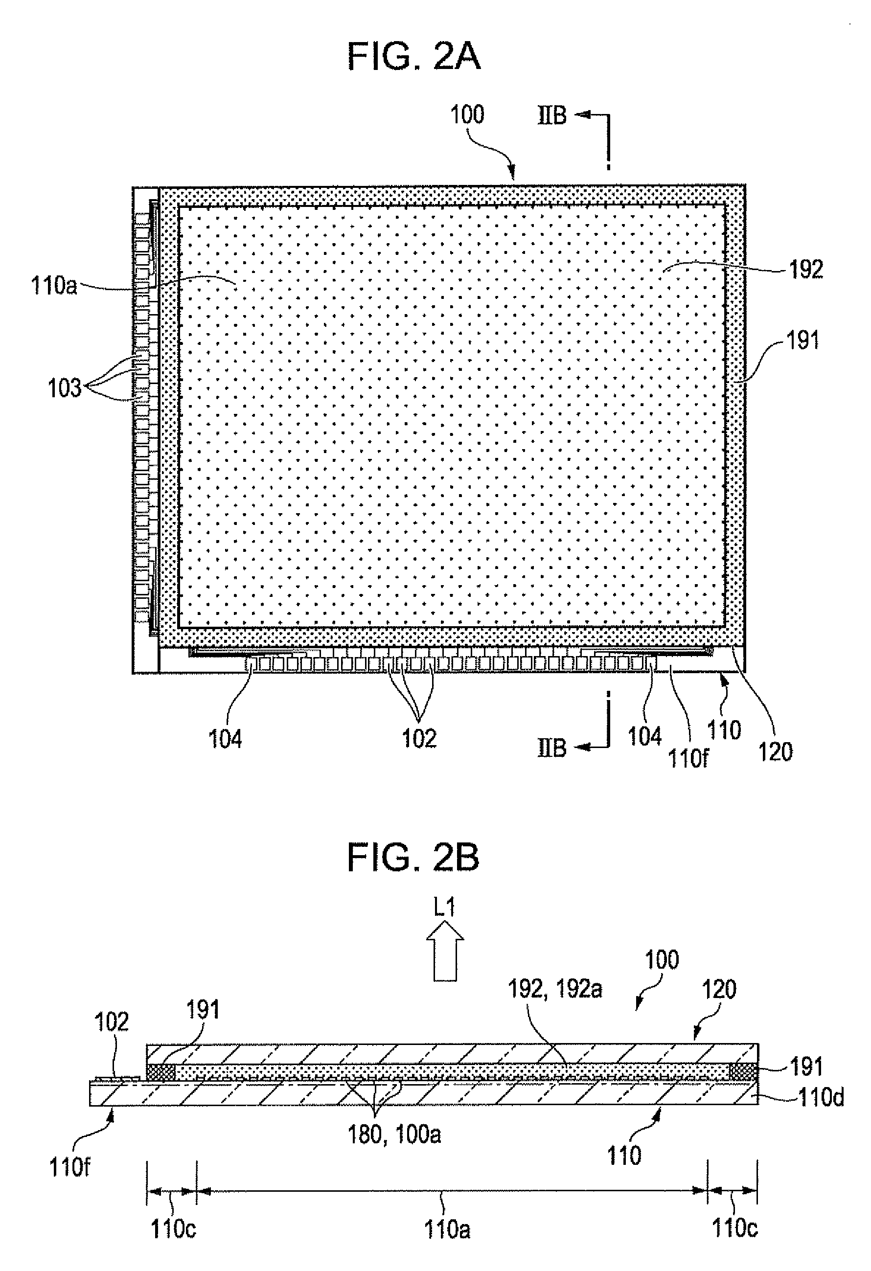
[0045]FIG. 1 is a block diagram showing an electrical structure of an organic EL device of the invention. FIG. 2A is a plan view of an organic EL device of the invention when viewed from a second substrate (sealing substrate) side, and FIG. 2B is a cross-sectional view taken along the line IIB-IIB shown in FIG. 2A.

[0046]An organic EL device 100 shown in FIG. 1 has a first substrate 110 used as an element substrate, a plurality of scanning lines 3a, a plurality of data lines 6a extending in a direction intersecting the scanning lines 3a, and pixels 100a provided at positions corresponding to the intersections between the scanning lines 3a and the data lines 6a, and a region in which the pixels 100a are disposed in a matrix forms a pixel region 110a.

[0047]In addition, on the first substrate 110, a plurality of power lines 6g extends parallel to the data lines 6a, and a plurality of capacity lines 3e extends parallel to the scanning lines 3a. A data line drive circuit 101 is connected...

embodiment 2

[0080]FIG. 6A is a schematic cross-sectional view of an organic EL device according to Embodiment 2 of the invention, and FIG. 6B is a schematic plan view of the first substrate 110 of the organic EL device shown in FIG. 6A, FIGS. 6A and 6B corresponding to FIGS. 3A and 3B, respectively, shown in Embodiment 1. FIG. 7A is a schematic view illustrating a plan structure of an electrical connection portion between a terminal and auxiliary wires (second electrode layer) on the first substrate 110 of the organic EL device according to Embodiment 2 of the invention, and FIG. 7B is a cross-sectional view taken along the line VIIB-VIIB shown in FIG. 7A, FIGS. 7A and 7B corresponding to FIGS. 5A and 5B, respectively, shown in Embodiment 1. Since the basic structure of this embodiment is similar to that of Embodiment 1, like elements are designated by the same reference numerals and a description thereof will be omitted.

[0081]As shown in FIGS. 6A, 6B 7A, and 7B, also in the organic EL device 1...

embodiment 3

[0086]FIG. 8A is a schematic cross-sectional view of an organic EL device according to Embodiment 3 of the invention, and FIG. 8B is a schematic plan view of the first substrate 110 of the organic EL device shown in FIG. 8A, FIGS. 8A and 8B corresponding to FIGS. 3A and 3B, respectively, shown in Embodiment 1. FIG. 9A is a schematic view illustrating a plan structure of an electrical connection portion between a terminal and auxiliary wires (second electrode layer) on the first substrate 110 of the organic EL device according to Embodiment 3 of the invention, and FIG. 9B is a cross-sectional view taken along the line IXB-IXB shown in FIG. 9A, FIGS. 9A and 9B corresponding to FIGS. 5A and 5B, respectively, shown in Embodiment 1. Since the basic structure of this embodiment is similar to that of each of Embodiment 1 and 2, like elements are designated by the same reference numerals and a description thereof will be omitted.

[0087]As shown in FIGS. 8A, 8B, 9A, and 9B, also in the organi...


PUM


Abstract

An organic electroluminescent device includes a pixel region in which a plurality of pixels is disposed on a support substrate, each pixel having an electroluminescent element in which at least a first electrode layer, a light-emitting layer, and a second electrode layer are laminated in that order at an upper layer side of an insulating film; a first conductive pattern portion provided at a lower layer side of the insulating film for applying a potential to the second electrode layer; and a second conductive pattern portion which is composed of a conductive film having a sheet resistance lower than that of the second electrode layer and which is provided at the upper layer side of the insulating film to connect the second electrode layer to the first conductive pattern portion. In this organic EL device, the second conductive pattern portion has a third conductive pattern portion which is provided on an upper surface of the first conductive pattern portion at a contact portion composed of a non-forming region of the insulating film and which is in contact with the first pattern portion.

Description

BACKGROUND[0001]1. Technical Field[0002]The present invention relates to an organic electroluminescent device (hereinafter referred to as an “organic EL device”) including organic electroluminescent elements (hereinafter referred to as “organic EL elements”) provided on a support substrate and an electronic apparatus including the above organic El device.[0003]2. Related Art[0004]Organic EL devices each have a pixel region in which a plurality of pixels is arranged on a support substrate, and in each of the plurality of pixels, an organic EL element is formed which includes at least a first electrode layer, a light-emitting layer, and a second electrode layer provided in that order at an upper layer side of an insulating film. Among the organic EL devices as described above, in particular, in a top emission-type organic EL device in which light emitted from an organic EL element is emitted through a second electrode layer, since the second electrode layer is required to have light t...

Claims


Application Information

Patent Timeline
IPC IPC(8): H01J1/62
CPCH01L27/3276H10K59/131
Inventor SHINTO, SUSUMU
Owner SEIKO EPSON CORP
Why Eureka
Try Eureka