Solar Cell

a solar cell and chalcopyrite technology, applied in the field of chalcopyrite solar cells, can solve the problems of inapplicability of mass production such as roll-to-roll process, inconvenient handling of products, and increased manufacturing facility size, so as to prevent any breakage of substrates, reduce the inner electrical resistance of series connections, and high reliability

Inactive Publication Date: 2009-10-01
HONDA MOTOR CO LTD
View PDF5 Cites 15 Cited by
  • Summary
  • Abstract
  • Description
  • Claims
  • Application Information

AI Technical Summary

Benefits of technology

[0032]With use of a substrate having flexibility, a solar cell of the present invention uses an electrode which is obtained by modifying a light absorber layer as an electrode for connecting a transparent conducting oxide layer and a lower electrode layer so that any breakage of the substrate can be prevented, and the inner electrical resistance of the connection in series can be reduced, thereby a highly reliable chalcopyrite solar cell can be obtained which has a high photoelectric conversion efficiency and no aged deterioration.
[0033]In addition, when a mica sheet substrate is used as the flexible substrate, a middle layer which contains a ceramic material may be provided between the mica sheet substrate and the lower electrodes to make a surface roughness of the substrate smooth like that of a glass substrate. The mica substrate contains potassium as an impurity which reduces a photoelectric conversion efficiency of the substrate, but a nitride-based binder layer may be provided to limit the diffusion of potassium to that of a glass substrate or less.

Problems solved by technology

On the contrary, a glass substrate has a low melting point, and it is difficult to set a high temperature for annealing in a gas phase selenidation step of the substrate, which resulting in a number of drawbacks including photoelectric conversion efficiency, an increased size of facility for manufacturing due to a large thickness and volume of the substrate, the inconvenience in handling of its product due to an increased weight of a module of the substrates, and the inapplicability of mass production such as roll-to-roll process due to little flexibility of the substrate.
Also, the thin connections between the unit cells are easily broken by an external force and aged deterioration, which results in a reduced reliability.
Furthermore, in addition to the above described common problems, the strength control of scribing using a metal needle or a laser beam to remove only a light absorber layer is difficult, and a too strong scribing breaks a lower electrode (Mo electrode).
A too weak scribing cannot completely remove a light absorber layer and leaves some which forms a layer having a high resistance, thereby causing a problem that a contact resistance between an upper transparent conducting oxide (TCO) and a lower Mo electrode is extremely increased.
Also the use of a metal needle requires replacing due to wear for example, which caused a problem that the maintenance is troublesome.
In addition, when a metal needle is used, there is a big problem in using flexible substrates described in Patent Documents 1 to 3.
Also, when a tungsten substrate, a nickel substrate, a graphite substrate, a stainless steel substrate or the like is used, the conductive substrate requires an insulation layer formed of SiO2 or the like, but a scribing of the substrate also cuts the insulation layer, which does not allow a formation of a monolithic connection in series.

Method used


Image

  • Solar Cell
  • Solar Cell
  • Solar Cell

Examples


Embodiment Construction

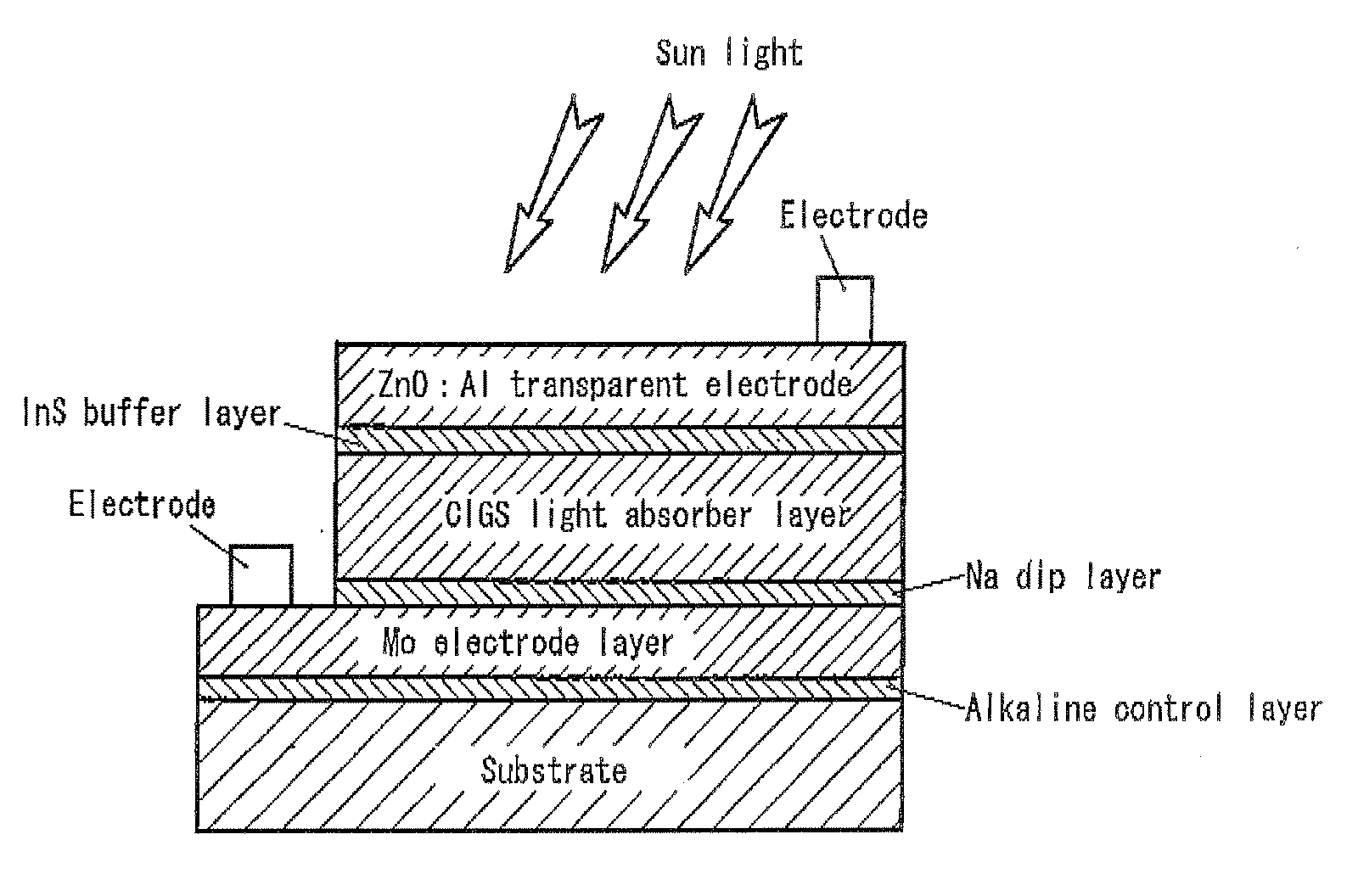
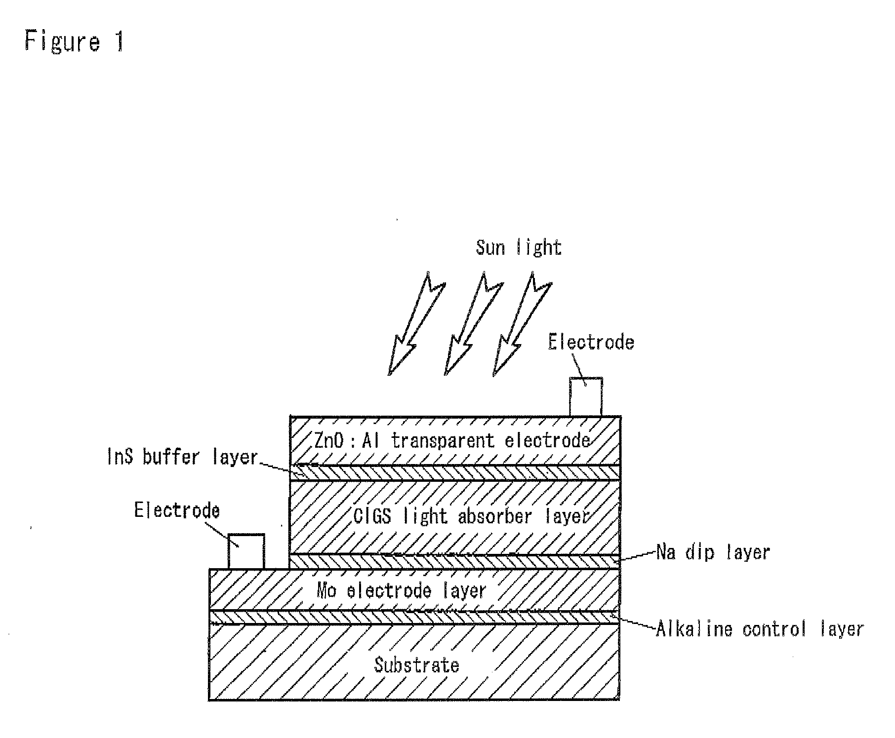
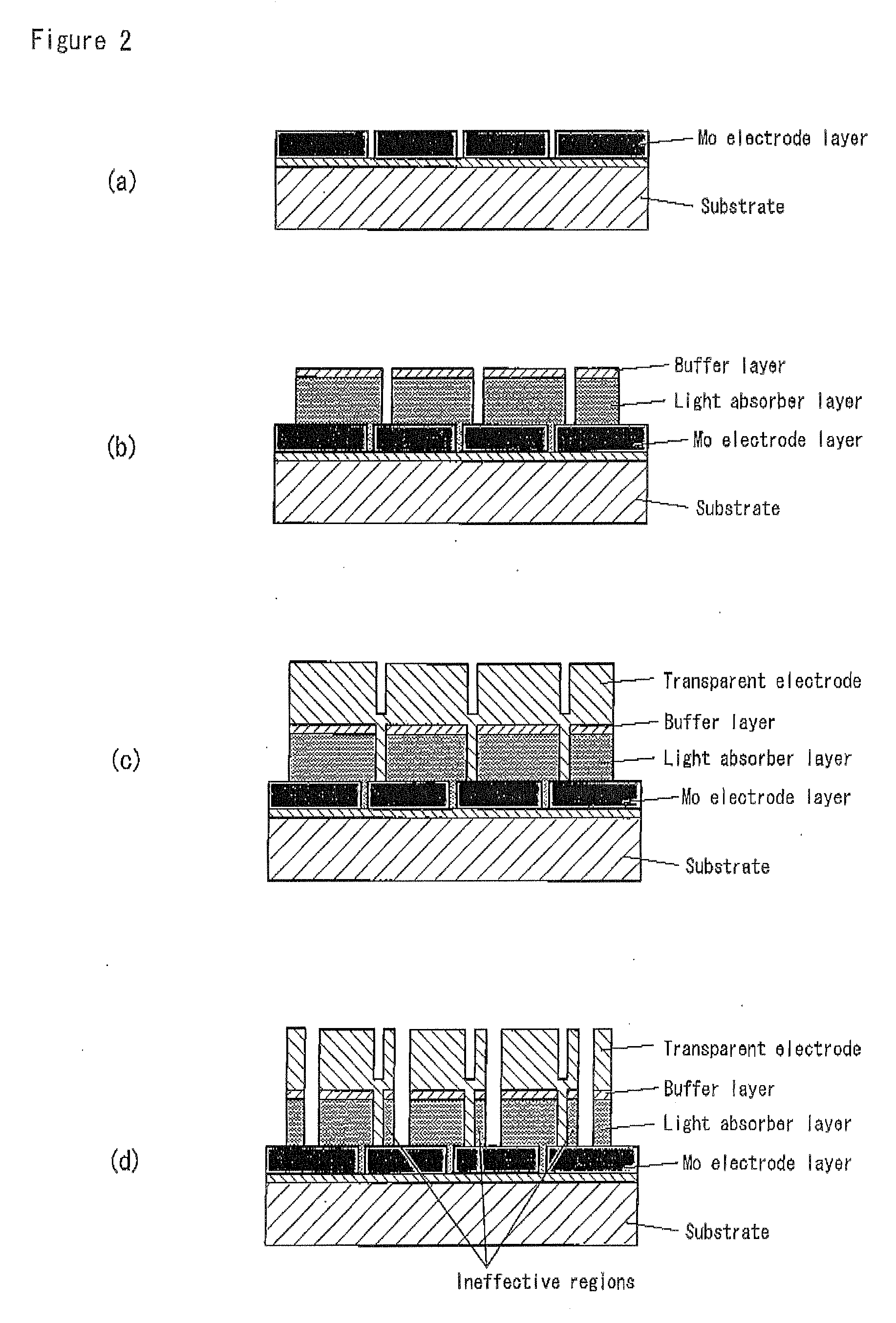
[0045]A chalcopyrite solar cell according to the present invention is shown in FIG. 5. FIG. 5(a) is a cross sectional view showing main sections of a solar cell (cell), and FIG. 5(b) is a view separately illustrating unit cells which comprise a solar cell (cell).

[0046]In the solar cell, a cell 10 (unit cell) is formed as a unit, comprising: a lower electrode layer 2 (Mo electrode layer) formed on a flexible substrate 1 (substrate); a light absorber layer 3 (CIGS light absorber layer) which contains copper-indium-gallium, and selenide; a highly resistant buffer layer thin film 4 formed of InS, ZnS, CdS, or the like on the light absorber layer 3; and an upper electrode layer 5 (TCO) formed of ZnOAl or the like, and furthermore, a contact electrode section 6 for connecting between the upper electrode layer 5 and the lower electrode layer 2 is formed in order to connect a plurality of unit cells 10 in series.

[0047]The contact electrode section 6 hasp as will be explained later, a Cu / In ...


PUM

PropertyMeasurementUnit
insulation resistanceaaaaaaaaaa
thicknessaaaaaaaaaa
wavelengthaaaaaaaaaa

Abstract

A flexible solar cell is achieved which has a high photoelectric conversion efficiency and no aged deterioration. A cell 10 (unit cell) is formed as a unit, comprising: a lower electrode layer 2 (Mo electrode layer) formed on a flexible mica sheet substrate 1 (substrate); a light absorber layer 3 (CIGS light absorber layer) which contains copper indium gallium selenide; a highly resistant buffer layer thin film 4 formed of InS, ZnS, CdS, or the like on the light absorber layer 3; and an upper electrode layer 5 (TCO) formed of ZuOAl or the like, and furthermore, a contact electrode section 6 for connecting between the upper electrode layer 5 and the lower electrode layer 2 is formed in order to connect a plurality of unit cells 10 in series. The contact electrode section 6 has a Cu/In ratio higher than that of the light absorber layer 3, and in other words, has less In contained therein to have a property of p+ (plus) type or a conductor relative to the light absorber layer 3 which is a p-type semiconductor.

Description

TECHNICAL FIELD[0001]The present invention relates to a chalcopyrite solar cell which is a compound solar cell, and more specifically relates to a solar cell using a flexible substrate and having an electrode connecting an upper electrode and a lower electrode.BACKGROUND ART[0002]Solar cells which receive light for converting it into an electrical energy are categorized into bulk solar cells and thin film solar cells depending on the thickness of semiconductor thereof. Between the two, the thin film solar cells have a semiconductor layer having a thickness of several tens μm to several μm or less, which are further categorized into Si thin film solar cells and compound thin film solar cells. The compound thin film solar cells include II-VI compound based solar cells and chalcopyrite based solar cells for example, which have been manufactured as several products already. Among them, chalcopyrite solar cells in the chalcopyrite based solar cells are also called CIGS (Cu(InGa)Se) thin ...

Claims


Application Information

Patent Timeline
Patent Type & Authority Applications(United States)
IPC IPC(8): H01L31/00H01L31/0392H01L31/0465H01L31/0749H01L51/42
CPCB23K26/367B23K26/409B23K2203/12H01L31/046H01L31/0336Y02E10/549H01L31/022466B23K26/364B23K26/40H01L31/0463Y02E10/541B23K2103/12B23K2103/172Y02P70/50
Inventor YONEZAWA, SATOSHI
Owner HONDA MOTOR CO LTD
Why Eureka
Try Eureka