Display device having touch panel

a display device and touch panel technology, applied in the field of touch panel display devices, can solve the problems of touch panel manufacturing cost and touch panel manufacturing cost of display devices, and achieve the effect of reducing the cost of the display device having a touch panel

Active Publication Date: 2009-08-13
JAPAN DISPLAY INC
View PDF9 Cites 53 Cited by
  • Summary
  • Abstract
  • Description
  • Claims
  • Application Information

AI Technical Summary

Benefits of technology

[0021]To briefly explain advantageous effects which are obtained by typical invention among inventions disclosed in this application, they are as follows.
[0022]According to the present invention, it is possible to realize the reduction of cost of the display device having a touch panel.

Problems solved by technology

Accordingly, the accurate alignment is necessary for connecting the lines formed on the substrate and the bump electrodes of the semiconductor chip and this accurate alignment pushes up a manufacturing cost of the touch panel and, eventually, a manufacturing cost of a display device having a touch panel.

Method used


Image

  • Display device having touch panel
  • Display device having touch panel
  • Display device having touch panel

Examples


embodiment 1

[0034]In the embodiment 1, the explanation is made with respect to an example in which the present invention is applied to a display device having a touch panel which mounts a touch panel on an organic EL display panel as one example of a display panel, for example.

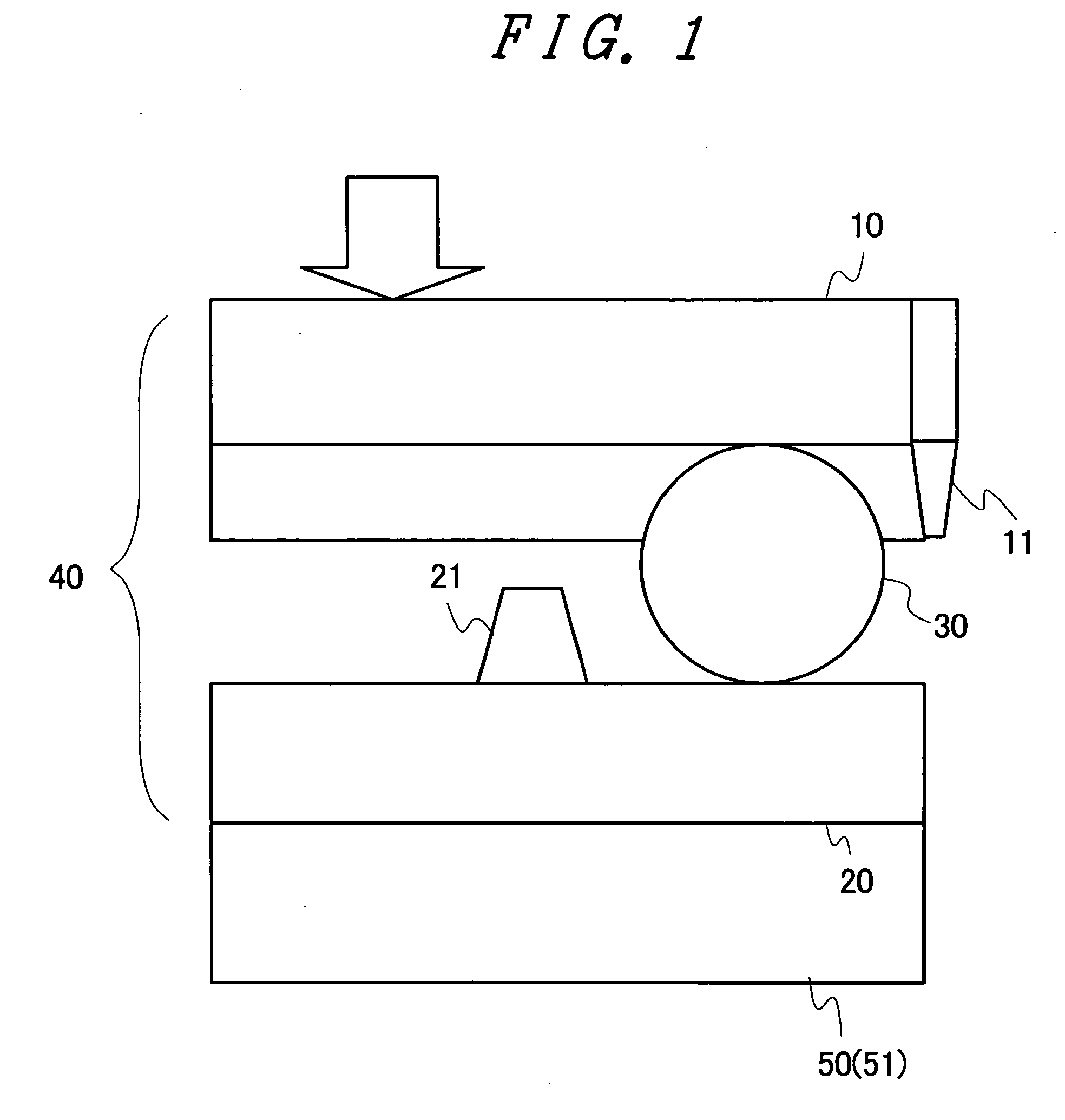
[0035]FIG. 1 is a cross-sectional view of the display device having a touch panel of the embodiment 1 according to the present invention.

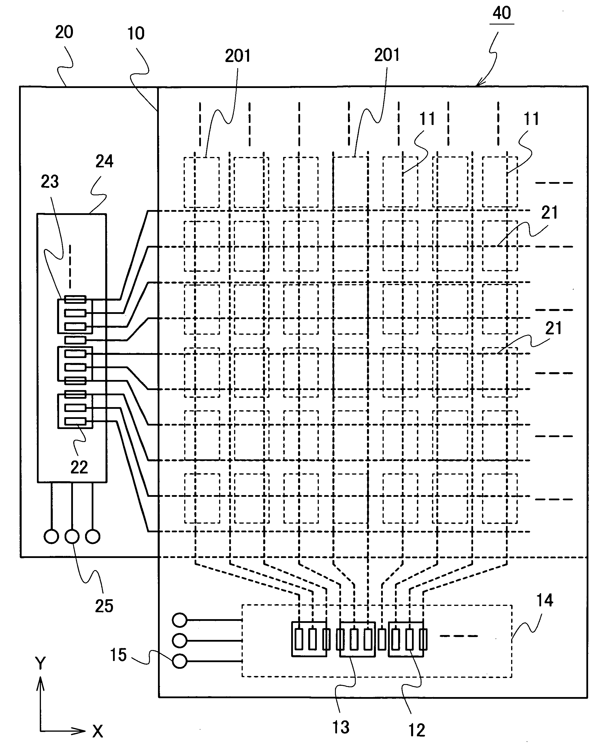
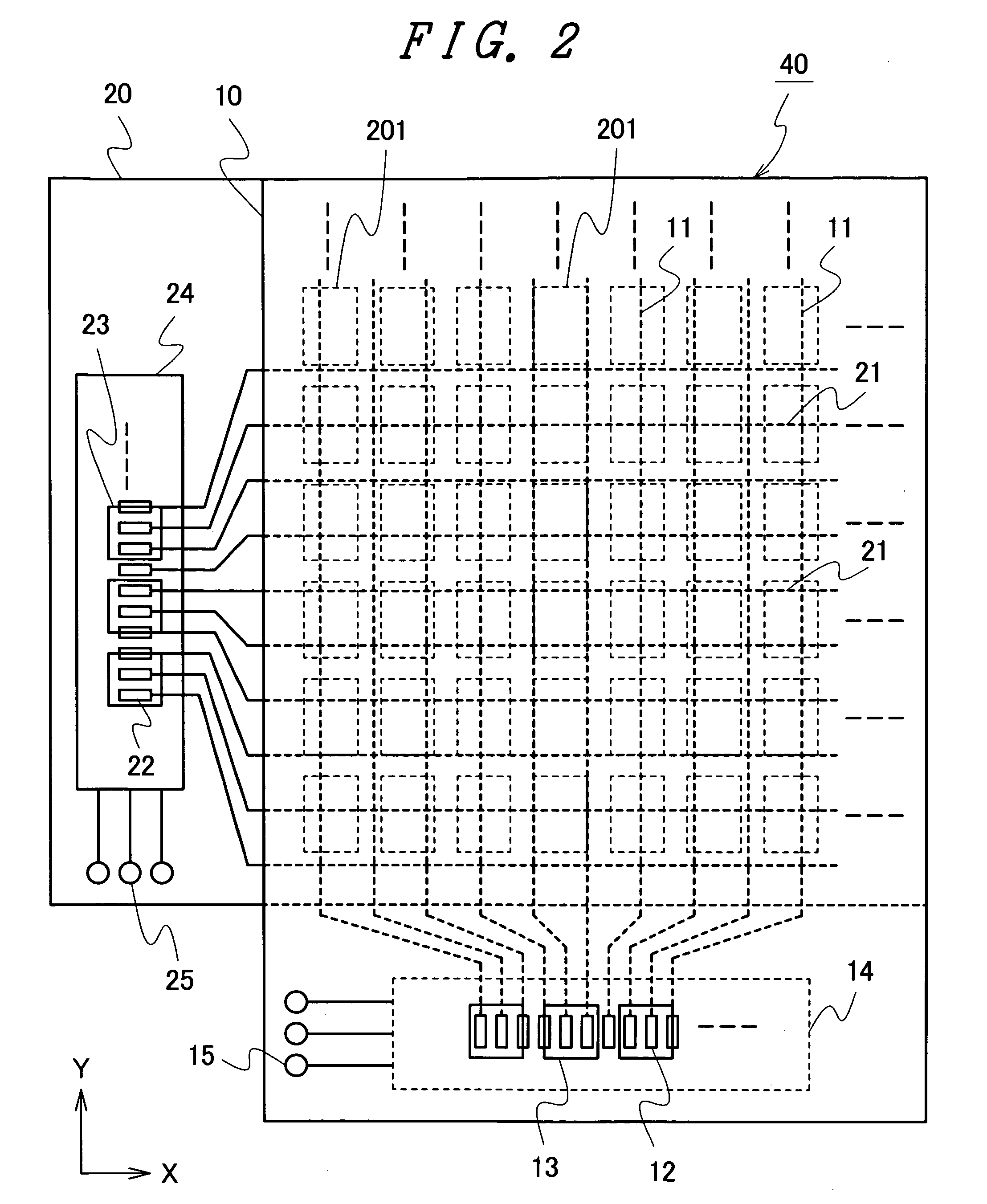
[0036]As shown in FIG. 1, the display device having a touch panel of the embodiment 1 includes a display panel 50, and a touch panel 40 which is arranged on the display panel 50 in an overlapping manner in plane. In this embodiment, an organic EL display panel 51 is adopted as the display panel 50, for example, and the touch panel 40 is arranged on the organic EL display panel 51.

[0037]FIG. 8 is a block diagram of a display part of the display panel (organic EL display panel) shown in FIG. 1.

[0038]As shown in FIG. 8, in the display part (display screen) of the organic EL display panel 51...

embodiment 2

[0087]FIG. 10 is a cross-sectional view of a display device having a touch panel of an embodiment 2 according to the present invention.

[0088]The basic structure and the manner of operation of the embodiment 2 of the present invention are substantially equal to the above-mentioned structure and manner of operation of the embodiment 1 and hence, their repeated explanation is omitted. The difference between the embodiment 1 and the embodiment 2 lies in the arrangement structure of the lines 11 and the lines 21 and hence, the structure of the lines 11 and the lines 21 is explained in conjunction with FIG. 10.

[0089]Lines 11A which are formed of a conductive body such as copper or STAINLESS STEEL are linearly arranged on a first substrate 10. Further, Lines 21A which are formed of a conductive body such as copper or STAINLESS STEEL are linearly arranged on a second substrate 20. Spacers 30 are interposed between the first substrate 10 and the second substrate 20. When a pressure is applie...


PUM


Abstract

The present invention realizes the reduction of cost of a display device having a touch panel. The display device having a touch panel includes a display panel, and a touch panel which is arranged on the display panel in an overlapping manner in plane. The touch panel includes a first substrate and a second substrate which are arranged to face each other with spacers sandwiched therebetween, and a first semiconductor chip which is mounted on the first substrate. The first substrate includes, on a surface side thereof which faces the second substrate, a plurality of first lines which is arranged parallel to each other in the first direction, a first chip mounting region on which the first semiconductor chip is mounted, and a plurality of first connection portions each of which is constituted of a portion of each line in the plurality of first lines, the first semiconductor chip includes a plurality of first bump electrodes which is arranged in one direction, the plurality of first connection portions are arranged in the arrangement direction of the plurality of first bump electrodes within the first-chip mounting region, and an arrangement pitch of the plurality of first bump electrodes is set larger than an arrangement pitch of the plurality of first connection portions.

Description

CROSS-REFERENCE TO RELATED APPLICATIONS[0001]The present application claims priority from Japanese Application JP 2008-31915 filed on Feb. 13, 2008, the content of which is hereby incorporated by reference into this application.BACKGROUND OF THE INVENTION[0002]1. Field of the Invention[0003]The present invention relates to a display device having a touch panel, and more particularly to a display device having a touch panel which mounts a touch panel on a display panel.[0004]2. Description of the Related Art[0005]As a detection method of a conventional touch panel, a detection method which detects a change of light and a detection method which detects a change of an electric property have been mainly used. With respect to a detection method which detects a change of an electric property, conventionally, a resistance film method and a capacitance method have been known. Further, before the advent of the resistance film method, as described in JP-A-2002-342014 (patent document 1), ther...

Claims


Application Information

Patent Timeline
Patent Type & Authority Applications(United States)
IPC IPC(8): G06F3/041
CPCG06F3/0412G06F3/041G06F3/047
Inventor AKIMOTO, HAJIMEYATSU, YASUHARUKAGEYAMA, HIROSHIMATSUDATE, NORIHARUKASAI, NARUHIKO
Owner JAPAN DISPLAY INC
Why Eureka
Try Eureka