Flat panel display device

a display device and flat panel technology, applied in the direction of instruments, mechanical devices, machine supports, etc., can solve the problems of shortening the processing time, affecting the accuracy of the display device, and limiting the thickness of the bezel

Inactive Publication Date: 2009-08-27
SAMSUNG DISPLAY CO LTD
View PDF6 Cites 65 Cited by
  • Summary
  • Abstract
  • Description
  • Claims
  • Application Information

AI Technical Summary

Problems solved by technology

However, the thickness of the bezel is limited, and must be kept smaller due to the trend toward slim display devices.
Moreover, the tape is m

Method used


Image

  • Flat panel display device
  • Flat panel display device
  • Flat panel display device

Examples


exemplary embodiment 1

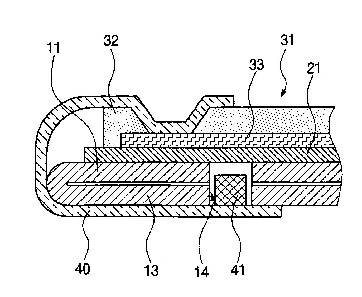
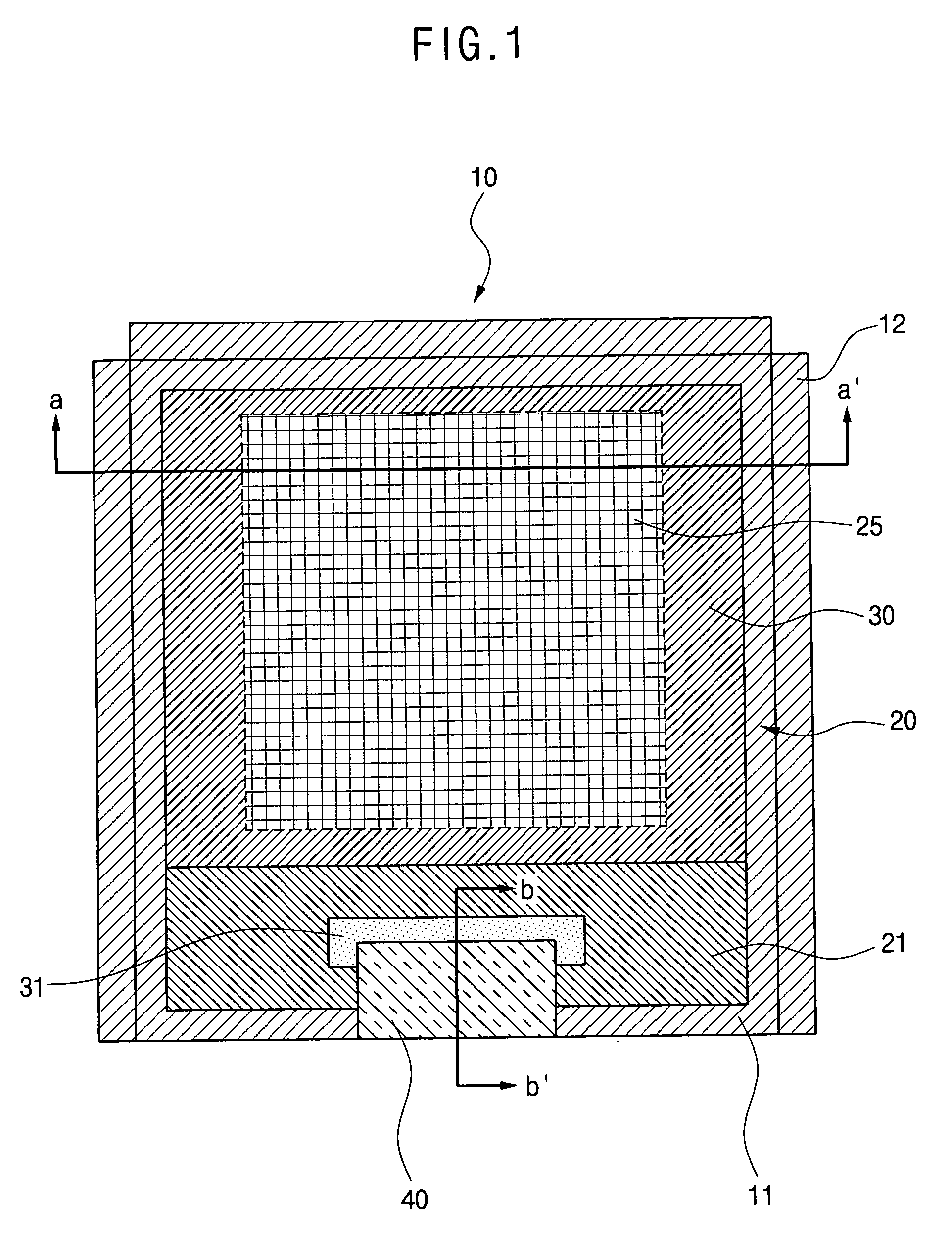
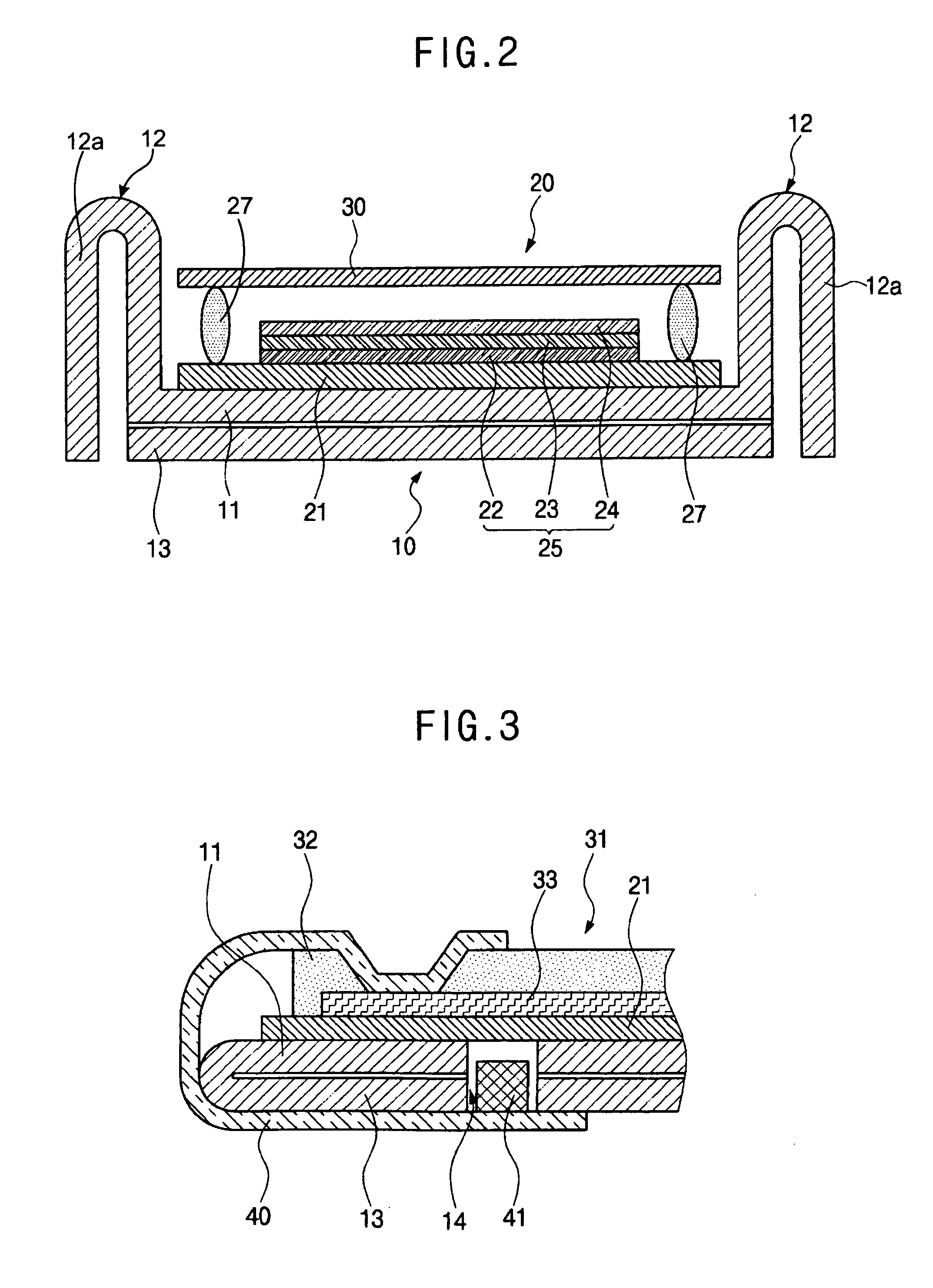
[0018]FIG. 1 is a plan view according to a first exemplary embodiment of the present invention, and FIG. 2 is a cross-sectional view taken along line a-a′ of FIG. 1.

[0019]Referring to FIGS. 1 and 2, a flat panel display device includes a bezel 10, a flat display panel 20 and a flexible printed circuit board (FPCB) 40.

[0020]The bezel 10 includes a first substrate part 11 supporting the flat display panel 20, and a second substrate part 13 which extends from one side of the first substrate part 11 and is folded.

[0021]The first substrate part 11 is bent at both edges in the same direction, thereby forming bent parts 12. Thus, the first substrate part 11 and the bent parts 12 may be formed of the same material.

[0022]The first substrate part 11 serves as a frame supporting and fixing the flat display panel 20. The first substrate part 11 is generally formed of a conductive metallic material, and is connected to the flat display panel 20 and a ground terminal of the FPCB 40, so that elect...

exemplary embodiment 2

[0046]FIG. 5 is a cross-sectional view of a flat panel display device according to a second exemplary embodiment of the present invention.

[0047]Referring to FIGS. 1 and 5, a flat panel display device includes a bezel 10, a flat display panel 20 and an FPCB 40.

[0048]In the second exemplary embodiment of the present invention, the configuration is the same as for the first exemplary embodiment, except for the bezel of the flat panel display device, and thus a description thereof will be omitted except for the bezel.

[0049]Referring to FIG. 5, the bezel is formed in a three-layer structure including a first substrate part 11, a second substrate part 13 which extends from one side of the first substrate part 11 and is folded, and a third substrate part 15 which extends from one side of the second substrate part 13 and is folded.

[0050]At least one opening 14 is formed at a location where the first, second and third substrate parts 11, 13 and 15, respectively, correspond to one another.

[00...


PUM


Abstract

A flat panel display device includes a folded bezel formed in a multi-layer structure. The flat panel display device is formed so that an electronic component of a flexible printed circuit board may be inserted into at least one opening formed at a location where the layers of the bezel correspond to one another. Thus, the electronic component inserted into the opening of the bezel has improved durability against external interference and impact, and the number of components and the number of processes can be reduced.

Description

CLAIM OF PRIORITY[0001]This application makes reference to, incorporates the same herein, and claims all benefits accruing under 35 U.S.C. §119 from an application for Flat Panel Display earlier filed in the Korean Intellectual Property Office on the 21 Feb. 2008 and there duly assigned Serial No. 10-2008-0015823.BACKGROUND OF THE INVENTION[0002]1. Technical Field[0003]The present invention relates to a flat panel display device and, more particularly, to a flat panel display device including a bezel formed in a multi-layer structure.[0004]2. Related Art[0005]Generally, flat panel display (FPD) devices, such as a liquid crystal display (LCD) device, a field emission display (FED) device, and an organic light emitting diode (OLED) display device, are accommodated in a bezel which functions as a frame so as to mechanically and electrically protect the FPDs.[0006]In this regard, when an opening is formed in the bezel, and an electronic component of a flexible circuit board is inserted ...

Claims


Application Information

Patent Timeline
IPC IPC(8): G02F1/1333
CPCG02F1/1345G02F1/13452G02F2001/133322G02F2001/133334H01L51/5237G02F2202/28H01J29/86H01L27/3276G02F2201/503Y10S345/905Y10S248/917G02F1/133322G02F1/133334H10K59/131H10K59/87G02F1/1333H10K50/84
Inventor PARK, HONG-SIKLEE, SANG-HYUNKIM, DONG-HO
Owner SAMSUNG DISPLAY CO LTD
Why Eureka
Try Eureka