Flexible nanostructure electronic devices

a flexible nanostructure and electronic device technology, applied in the direction of nanoinformatics, discharge tube/lamp details, discharge tube luminescnet screens, etc., can solve the problems of low transconductance of these devices, extremely low carrier mobilities of organic materials, and slow flexible electronics

Active Publication Date: 2005-08-25
NANOMIX +1
View PDF16 Cites 135 Cited by
  • Summary
  • Abstract
  • Description
  • Claims
  • Application Information

AI Technical Summary

Problems solved by technology

The core problem with these previous developments has been that the organic materials have extremely low carrier mobilities.
As a result, the transconductance of these devices has been very small.
Since transconductance determines the speed of a device, flexible electronics have been very slow.
However, certain obstacles are encountered in the manipulation of these nano-electronic or microscopic objects.
The laying down of a thin film of nanotubes is not easily accomplished.
One difficulty arises from the fact that nanotubes have a very poor solubility in typical solvents without the use of surfactants, impeding film-forming using carrier solvents.
Furthermore, when nanotubes are suspended or dissolved in solution at low concentrations, evaporation (e.g., drying) of the carrier liquid may result in flocculation and clumping, when the local concentration of nanotubes approaches the solubility limit.
Moreover, surfactants that make the nanotubes compatible with aqueous dispersions may be inappropriate for applications that require pure nanotubes.
Under some situations, nanotubes can be deposited with spin coating, but for the thinnest films (<1 μm), it is difficult to get adequate uniformity.

Method used


Image

  • Flexible nanostructure electronic devices
  • Flexible nanostructure electronic devices
  • Flexible nanostructure electronic devices

Examples


example a

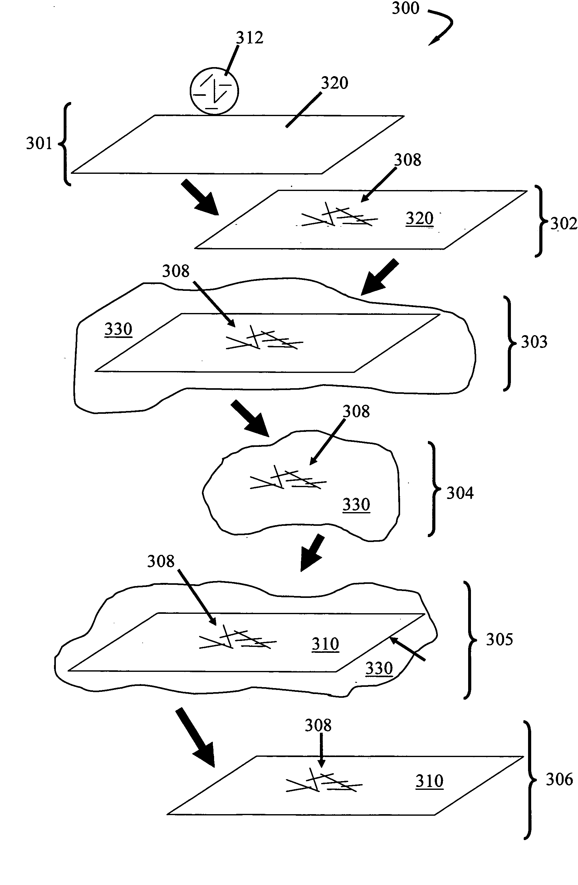
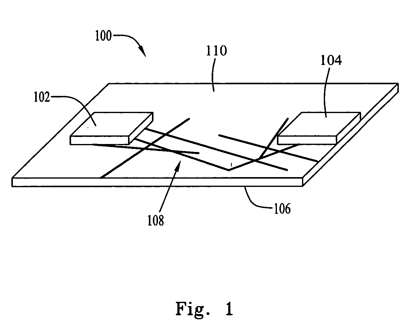
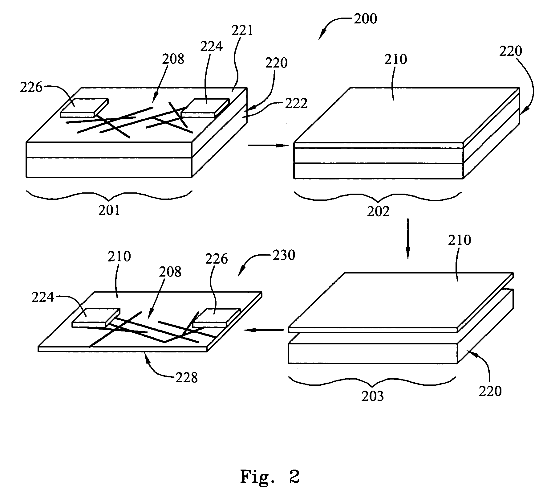
[0044] A nanotube network was grown by chemical vapor deposition on a silicon substrate with a 200 nm silicon oxide coating, as described in U.S. patent application Ser. No. 10 / 177,929, filed Jun. 21, 2002 by Gabriel et al., which is hereby incorporated by reference, in its entirety. Then the silicon substrate with the network was patterned with optical lithography, and a liftoff process, to form 100 μm square metal contacts. The metal contacts comprised a 3.5 nm thick titanium film covered by a 50 nm thick gold film. After liftoff, the silicon substrate with network and metal contacts was spin-coated with polyimide (HD 2610, 500 rpm). The silicon substrate was heated at 90° C. for 10 minutes, 120° C. for 5 minutes, and 200° C. for 30 minutes to cure the polyimide. Finally, the silicon substrate was immersed in 10% hydrofluoric acid (HF) for 8 hours. The polyimide films, floating freely in the HF solution, were removed and rinsed with deionized water.

[0045] A device on a flexible s...

example b

[0047] A nanotube solution was made using nanotubes grown by laser ablation. To make the solution, nanotubes were dispersed in 10:1 dimethylbenzene:dichlorobenzene solution using a high-powered ultrasonicator. The concentration of nanotubes was between 1 mg / L and 5 mg / L. The solution was placed on an alumina membrane (Whatman, 0.2 μm pore size), and a pump was used to draw the solvent through the membrane. A uniform nanotube film was found deposited on the membrane. While the membrane was still damp with solvent, a chamber underneath the membrane was filled with deionized water. When the water reached the membrane, the nanotube film was observed to float free of the membrane. The film floated on the water surface in the form of large rafts. At this point, the device substrate was slipped into the water under the rafts, then the pump was used to remove the water. As the water disappeared, the rafts were redeposited on the substrate.


PUM

PropertyMeasurementUnit
concentrationaaaaaaaaaa
pore sizeaaaaaaaaaa

Abstract

A flexible electronic device is made up of nanostructures. Specifically, the device includes a flexible substrate, a film of nanostructures in contact with the flexible substrate, a first conducting element in contact with the film of nanostructures, and a second conducting element in contact with the film of nanostructures. The nanostructures may comprise nanotubes, such as carbon nanotubes disposed along the flexible substrate, such as an organic or polymer substrate. The first and second conductive elements may serve as electrical terminals, or as a source and drain. In addition, the electronic device may include a gate electrode that is in proximity to the nanotubes and not in electrical contact with the nanotubes. In this configuration, the device can operate as a transistor or a FET. The device may also be operated in a resistive mode as a chemical sensor (e.g., for sensing NH3).

Description

CROSS-REFERENCE TO RELATED APPLICATION [0001] This application claims priority pursuant to 35 U.S.C. § 119(e) to U.S. Provisional Application No. 60 / 471,243, filed May 16, 2003, which application is specifically incorporated herein, in its entirety, by reference.BACKGROUND OF THE INVENTION [0002] 1. Field of the Invention [0003] The present invention relates to flexible nanostructure electronic devices, such as nanotube sensors and transistors, and method for fabricating the same. [0004] 2. Description of Related Art [0005] Flexible electronics or transistors are desirable for many applications. These applications include applications in flexible displays, wearable electronics, intelligent papers, and lightweight / cheap electronics. To meet these applications, it is important to have a flexible semiconducting channel. Many flexible transistors have been developed by using organic channels such as semiconducting polymers or organic crystals (e.g. crystalline pentane). The other elemen...

Claims


Application Information

Patent Timeline
Patent Type & Authority Applications(United States)
IPC IPC(8): H01B1/24H01J1/62H01J63/04H01L51/00
CPCB82Y10/00B82Y15/00H01L51/0595H01L51/0048H01L51/0097H01B1/24H10K85/221H10K10/701H10K77/111
Inventor ARMITAGE, N. PETERBRADLEY, KEITHGABRIEL, JEAN-CHRISTOPHE P.GRUNER, GEORGE
Owner NANOMIX
Why Eureka
Try Eureka