Hermetically-sealed packages for electronic components having reduced unused areas

Inactive Publication Date: 2009-09-03
CORNING INC
View PDF11 Cites 11 Cited by
  • Summary
  • Abstract
  • Description
  • Claims
  • Application Information

AI Technical Summary

Benefits of technology

[0016](e) at least one of Dfirst and Dsecond is less than or equal to 200 microns.
[0017]In certain embodiments, both Dfirst and Dsecond are less than or equal to 200 microns. In othe

Problems solved by technology

However, the organic molecules used in OLEDs are strongly reactive with oxygen and moisture, and thus susceptible to damage from exposure to air.
Such exposure may lead to a reduction in the useful life of the light emitting device.
The sintered frit sealing technique, however, does have the disadvantage that it uses a high power laser to melt the sintered frit.
The resulting thermal cycle can cause thermal damage to OLED devices, a problem which does not usually arise with epoxy sealing employing ultraviolet (UV) curing.
A further limitation on useable space arises from the manner in which OLED-containing glass packages are processed after laser sealing has been completed.
In practice, it has been found that if the score line is too close to the edges of the sintered frit, the frit will be exposed to a high level of stress during the scoring and breaking process which will weaken the bond strength significantly and / or cause delamination.
It is also difficult to achieve glass edges free of defects without damaging the sintered frit after scoring if the score line is too close to the sintered frit edge.
Small displays also present challenges with regard to strength since, as is well known, such displays are often dropped, sat on, bumped, and otherwise abused in the field.
However, given the limited areas available as a result of the inner and outer unused areas, dedicating more space to the sintered frit wall has been resisted by OLED display manufacturers.

Method used


Image

  • Hermetically-sealed packages for electronic components having reduced unused areas
  • Hermetically-sealed packages for electronic components having reduced unused areas
  • Hermetically-sealed packages for electronic components having reduced unused areas

Examples


Embodiment Construction

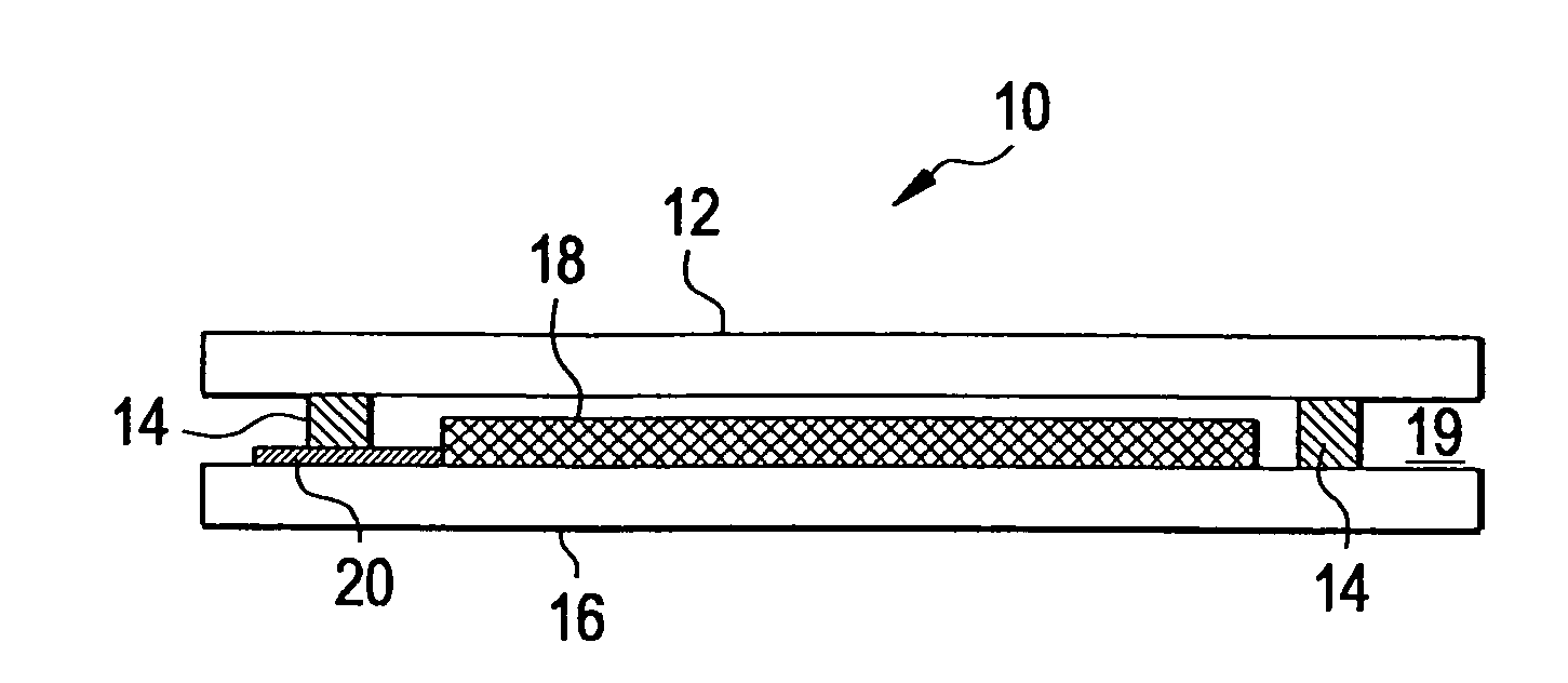
[0030]As discussed above, the present invention relates to the packaging of electronic components, e.g., temperature sensitive elements such as OLEDs, wherein the sealed and sized package has: (1) a high level of hermeticity and (2) a reduced unused area, specifically, a reduced outer unused area.

[0031]FIG. 1 is a schematic, cross-sectional, side view of a hermetically sealed OLED display device, generally designated by reference numeral 10, comprising a first substrate 12, a sintered frit pattern 14, a second substrate 16, at least one OLED element 18, and at least one electrode 20 in electrical contact with the OLED element. Typically, OLED element 18 is in electrical contact with an anode electrode and a cathode electrode. Electrode 20 in FIG. 1 is intended to represent either electrode. Although only a single OLED element is shown for simplicity, display device 10 may have many OLED elements disposed therein. The typical OLED element 18 includes one or more organic layers (not s...


PUM


Abstract

Hermetically-sealed packages for electronic components, e.g., OLEDs, are provided. The packages have a first glass substrate (12), a second glass substrate (16), and a wall (14) that separates the first and second substrates (12,16) and hermetically seals the electronic component (18) between the substrates (12,16). The package has a reduced outer unused area characterized by distances Dfirst (32a) and Dsecond (32b) at least one of which, and, in certain embodiments, both of which are less than 200 microns, e.g., one or both of Dfirst (32a) and Dsecond (32b) is approximately 100 microns. The reduction in unused area can be used to increase viewing area, improve electrical lead design, and / or increase package strength through the use of a wider sintered frit wall (14).

Description

I. FIELD OF THE INVENTION[0001]This invention relates to hermetically-sealed packages for electronic components, such as the organic light emitting diodes (OLEDs) used in displays. More particularly, the invention relates to hermetically-sealed packages having reduced unused areas and to methods for producing such packages.II. BACKGROUND OF THE INVENTION[0002]OLED-based displays are currently being considered for use in many applications which presently employ liquid crystal displays (LCDs). OLED-based displays can provide brighter and clearer images than liquid crystal displays and also need less power. However, the organic molecules used in OLEDs are strongly reactive with oxygen and moisture, and thus susceptible to damage from exposure to air. Such exposure may lead to a reduction in the useful life of the light emitting device. Therefore, hermetic sealing is one of basic requirements for long term performance of OLEDs.[0003]Efforts have been made to hermetically seal OLED-based...

Claims


Application Information

Patent Timeline
IPC IPC(8): B65D85/00
CPCH01L51/5237H01L21/67005H10K59/8722H05B3/04H10K50/8426
Inventor NGUYEN, KELVINHAASE PASTEL, MICHELLE NICOLEZHANG, LU
Owner CORNING INC
Why Eureka
Try Eureka