Flexible display

Active Publication Date: 2009-09-03
NANOLUMENS ACQUISITION
View PDF10 Cites 141 Cited by
  • Summary
  • Abstract
  • Description
  • Claims
  • Application Information

AI Technical Summary

Benefits of technology

[0016]Under an exemplary method of the present invention, multiple LEDs share a single LED substrate by cutting the LED wafer into larger units, chixels, that comprise a plurality of LEDs that define subpixels and together form pixels of a display. This allows for uniform spacing between the LEDs, and therefore uniform spacing between subpixels and pixels and results in smaller subpixel and pixel gaps. By manufacturing the LEDs on the same rigid wafer substrate, the pitch of the LEDs can be tightly controlled during the LED wafer manufacturing process using masking, etching and other techniques thereby providing a uniform subpixel and pixel pitch. The LEDs may be provided with contacts and a drive means to form workable subpixels of a display.
[0017]Furthermore, the exemplary method allows for different chixel sizes and shapes to be selected during the dicing process and is easily adjustable to different subpixel sizes by changing the etching process. For example, an LED wafer may be grown having LEDs of a size 320 microns square and separated by 320 microns on each side and then separated into sub-units of 96 LEDs, each LED corresponding to a subpixel of a display. For example, the 96 LEDs may correspond to 8 rows of 12 subpixels. The subpixels may be grouped into three to define pixels to form a 4×8 pixel

Problems solved by technology

It has proven difficult, however, to produce a large flexible display, as manufacturing techniques used to produce small-scale displays

Method used


Image

  • Flexible display
  • Flexible display
  • Flexible display

Examples


Embodiment Construction

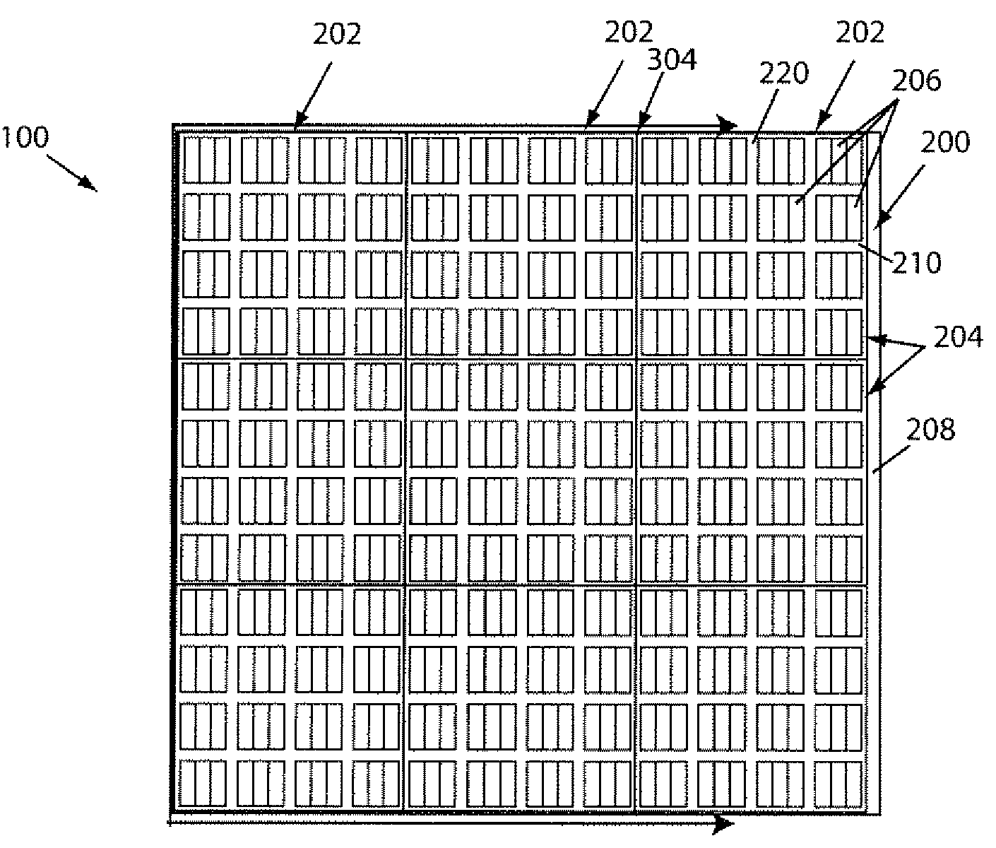
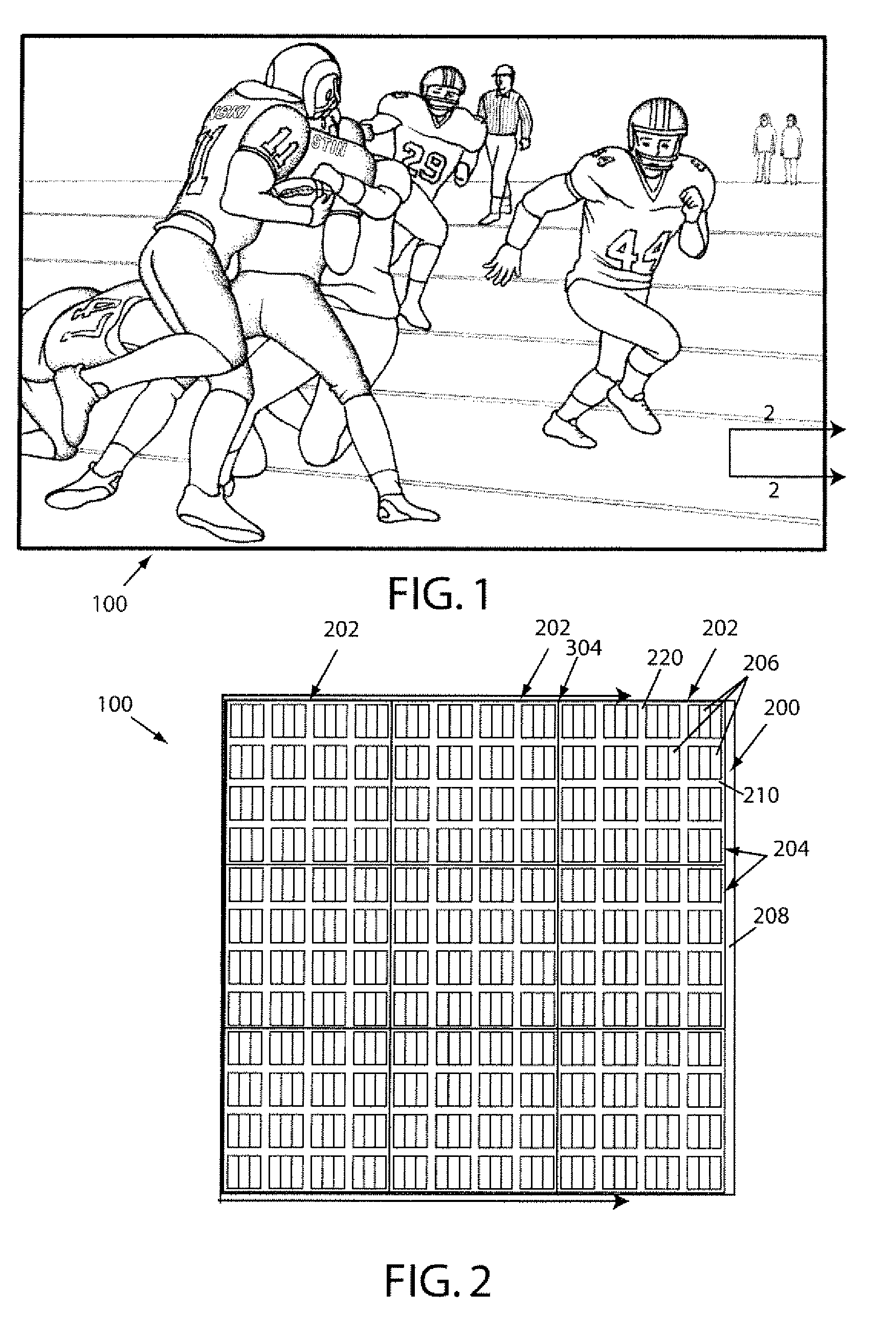
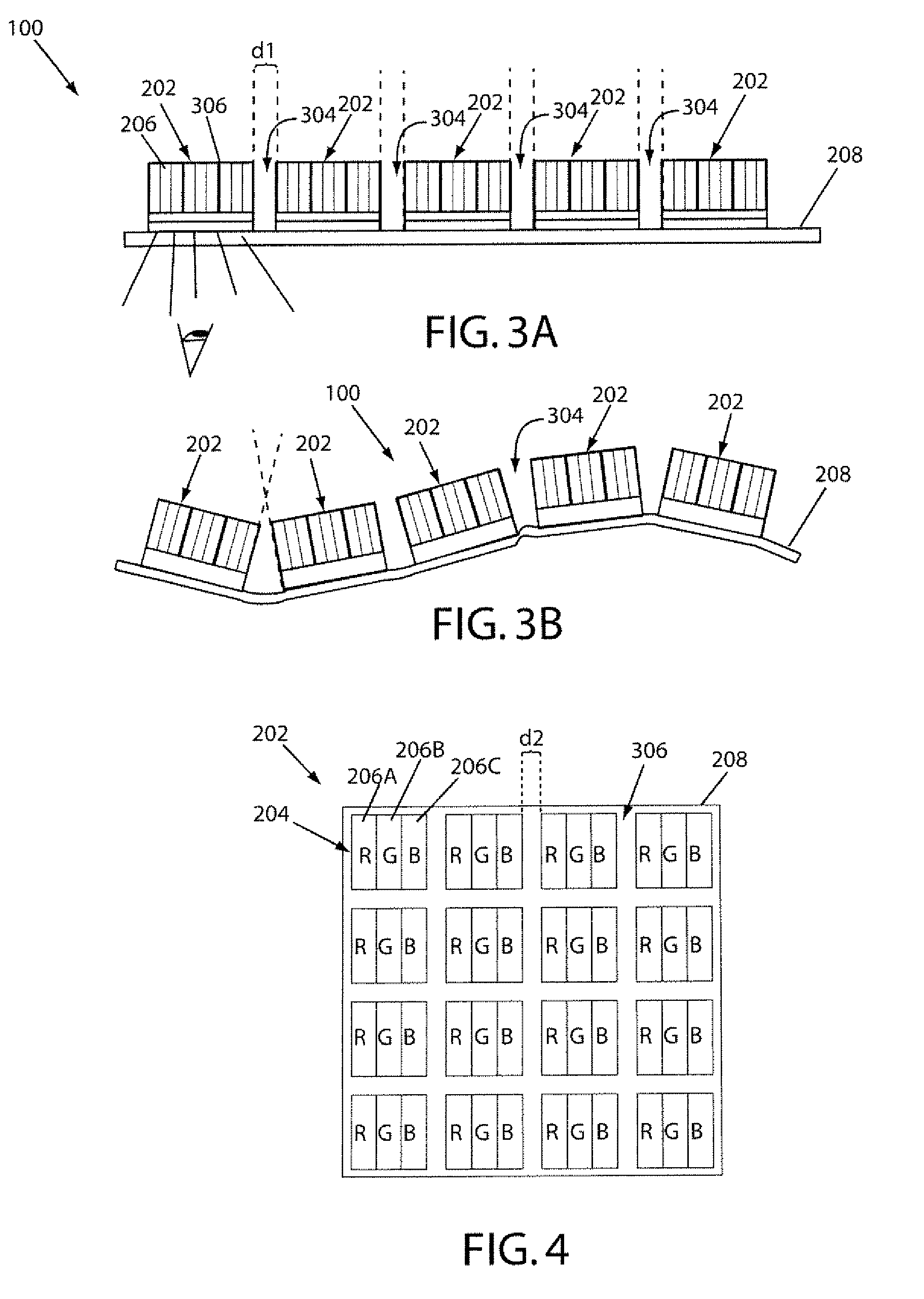
[0055]As required, exemplary embodiments of the present invention are disclosed herein. These embodiments are meant to be examples of various ways of implementing the invention and it will be understood that the invention may be embodied in alternative forms. The figures are not to scale and some features may be exaggerated or minimized to show details of particular elements, while related elements may have been eliminated to prevent obscuring novel aspects. Therefore, specific structural and functional details disclosed herein are not to be interpreted as limiting, but merely as a basis for the claims and as a representative basis for teaching one skilled in the art to variously employ the present invention.

[0056]For purposes of teaching and not limitation, the exemplary embodiments disclosed herein are discussed mainly in the context of LED light emitter technologies. However, the present invention is applicable to other light emitting technologies as well, such as, by way of exam...


PUM

PropertyMeasurementUnit
Flexibilityaaaaaaaaaa

Abstract

A flexible display includes a plurality of pixel chips, chixels, provided on a flexible substrate. The chixels and the light emitters thereon may be shaped, sized and arranged to minimize chixel, pixel, and subpixel gaps and to provide a desired bend radius of the display. The flexible substrate may include light manipulators, such as filters, light convertors and the like to manipulate the light emitted from light emitters of the chixels. The light manipulators may be arranged to minimize chixel gaps between adjacent chixels.

Description

CROSS REFERENCES TO RELATED APPLICATIONS[0001]This application claims priority to U.S. Provisional Patent Application No. 61 / 019,144 filed on Jan. 4, 2008.FIELD OF INVENTION[0002]The present invention relates to display devices. More particularly, the present invention comprises a flexible display.BACKGROUND[0003]There has been increased interest in the development of flexible displays. It has proven difficult, however, to produce a large flexible display, as manufacturing techniques used to produce small-scale displays have not proven readily scalable. Presently, large scale displays tend to be heavy, expensive, non-flexible, unreliable and power hungry.SUMMARY OF THE INVENTION[0004]In one exemplary embodiment, a flexible display includes a plurality of self-contained pixel-containing chips, called chixels, that are arranged on a flexible substrate in a manner that provides sufficient bend radius to the substrate to allow flexing of the display. The chixels may include a sub-array ...

Claims


Application Information

Patent Timeline
IPC IPC(8): G09G3/20
CPCG09F9/30G09F9/33G09G3/20G09G3/2088H01L2251/5338G09G2300/04G09G2300/0426G09G2300/0452G09G2380/02G09G3/32H01L2924/0002G09F9/301B05D3/0493B05D2252/02C23C14/562H01L31/03923H01L31/206Y02E10/541Y02P70/50G09G3/035H10K2102/311H01L2924/00H01L25/0753H01L33/20H01L33/483H01L23/4985H01L2933/0033H01L25/0655H01L27/153H01L33/32H01L33/48G06F3/1438G06F3/1446G09G2300/026G09G2320/0626G09G2380/06
Inventor COPE, RICHARD C.
Owner NANOLUMENS ACQUISITION
Why Eureka
Try Eureka