Solid-state imaging device and its manufacturing method

a technology of solid-state imaging and manufacturing methods, which is applied in the direction of instruments, television systems, lenses, etc., can solve the problems of deteriorating image quality, smear, and more likely leakage of electric charge into the charge transfer unit, so as to prevent smear and improve image quality. , the effect of high reliability

Inactive Publication Date: 2009-09-10
PANNOVA SEMIC
View PDF3 Cites 11 Cited by
  • Summary
  • Abstract
  • Description
  • Claims
  • Application Information

AI Technical Summary

Benefits of technology

[0009]According to examples of a solid-state imaging device and its manufacturing method disclosed herein, it is possible to reduce the amount of oblique incident light component entering the photoelectric conversion region, so that the deterioration of an image due to the occurrence of a smear can be suppressed.
[0011]With this configuration, a flat surface positioned immediately above the photoelectric conversion region is provided on at least one of the first and second microlenses. Therefore, external light can be gathered via the flat surface into the photoelectric conversion region. External light passing through the flat surface enters the photoelectric conversion region perpendicularly or at a relatively small angle of incidence, so that the light can be gathered into a middle portion of the photoelectric conversion region. As a result, in the solid-state imaging device of the present invention, it is possible to reduce the amount of oblique incident light entering the photoelectric conversion region. In other words, it is possible to suppress the situation that oblique incident light is converted into electricity in the vicinity of a charge transfer unit, and the resultant electric charge leaks into the charge transfer unit. As a result, the occurrence of a smear is suppressed, so that a solid-state imaging device having a satisfactory image characteristic can be achieved.
[0019]With this method, the first microlens having a flat surface positioned immediately above the photoelectric conversion region can be formed by step (e). Therefore, light entering the first microlens can be gathered via the flat surface into a middle portion of the photoelectric conversion region. Therefore, by using the solid-state imaging device manufacturing method, it is possible to reduce the amount of oblique incident light entering the photoelectric conversion region. As a result, the occurrence of a smear is suppressed, so that a solid-state imaging device having a satisfactory image characteristic can be achieved.
[0020]Note that, in step (d), a flat surface may be formed at a top portion of the second microlens and within the photoelectric conversion region as viewed from the top. In this case, a flat surface can be formed on the second microlens as well as on the first microlens, so that external light can be efficiently gathered via the flat surface of the second microlens and the flat surface of the first microlens into the photoelectric conversion region.
[0029]With this method, the second microlens having a flat surface positioned immediately above the photoelectric conversion region can be formed by step (l). Therefore, light entering the second microlens can be gathered via the flat surface into a middle portion of the photoelectric conversion region. Therefore, by using the solid-state imaging device manufacturing method, it is possible to reduce the amount of oblique incident light entering the photoelectric conversion region. As a result, the occurrence of a smear is suppressed, so that a solid-state imaging device having a satisfactory image characteristic can be achieved.
[0035]According to examples of a solid-state imaging device and its manufacturing method of the present invention, the incidence of oblique incident light into the photoelectric conversion region can be suppressed, so that a deterioration in an image due to a smear can be prevented. Therefore, even if the number of pixels is increased and a solid-state imaging device is further miniaturized, the solid-state imaging device can achieve high reliability.

Problems solved by technology

However, as the number of pixels of a solid-state imaging device is increased while the solid-state imaging device is miniaturized, electric charge is more likely to leak into a charge transfer unit, so that a smear occurs.
The smear degrades image quality.
For a Charge Coupled Device (CCD) for moving images, which cannot employ a mechanical shutter, it is not possible to remove a smear component remaining in a charge transfer unit, so that a deterioration in image quality due to the smear becomes significant.
In this case, oblique incident light is converted into electricity in the vicinity of a charge transfer unit, so that the resultant electric charge leaks into the charge transfer unit.
In this case, as described above, the oblique incident light is converted into electricity in the vicinity of a charge transfer unit, so that a smear occurs, leading to a deterioration in an image.

Method used


Image

  • Solid-state imaging device and its manufacturing method
  • Solid-state imaging device and its manufacturing method
  • Solid-state imaging device and its manufacturing method

Examples


first embodiment

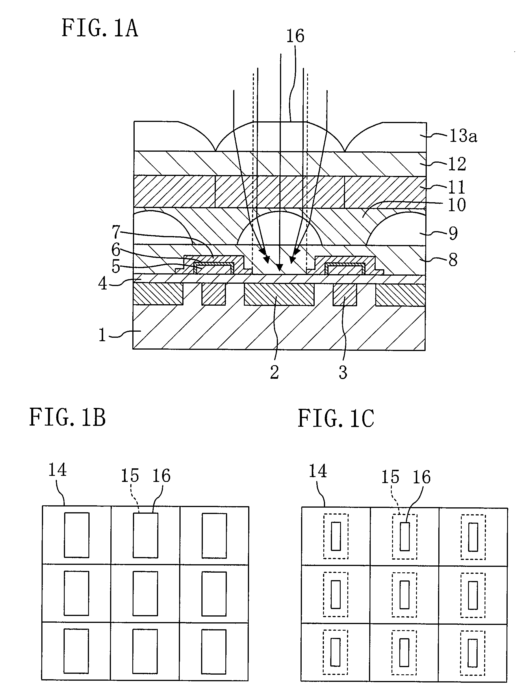
[0050]FIG. 1A is a cross-sectional view showing a configuration of a solid-state imaging device according to this embodiment. As shown in FIG. 1A, the solid-state imaging device of this embodiment includes: a semiconductor substrate 1 made of silicon or the like; a photoelectric conversion region (photoelectric conversion device region) 2 and a transfer channel region 3 provided in the semiconductor substrate 1; a first insulating film 4 provided on an entire surface of the semiconductor substrate 1; a transfer electrode 5 provided on the transfer channel region 3 with the first insulating film 4 being interposed therebetween; a second insulating film 6 covering a side surface and an upper surface of the transfer electrode 5; a light shield film 7 provided on the first insulating film 4, extending over a side surface and an upper surface of the second insulating film 6, and having an opening portion directly above the photoelectric conversion region 2; a first planarization layer 8 ...

second embodiment

[0056]FIG. 2A is a cross-sectional view showing a configuration of a solid-state imaging device according to a second embodiment of the present invention. Note that the solid-state imaging device of this embodiment is different from that of the first embodiment in only a portion of the configuration. Therefore, the same parts as those of the first embodiment are indicated by the same reference symbols and will not be described.

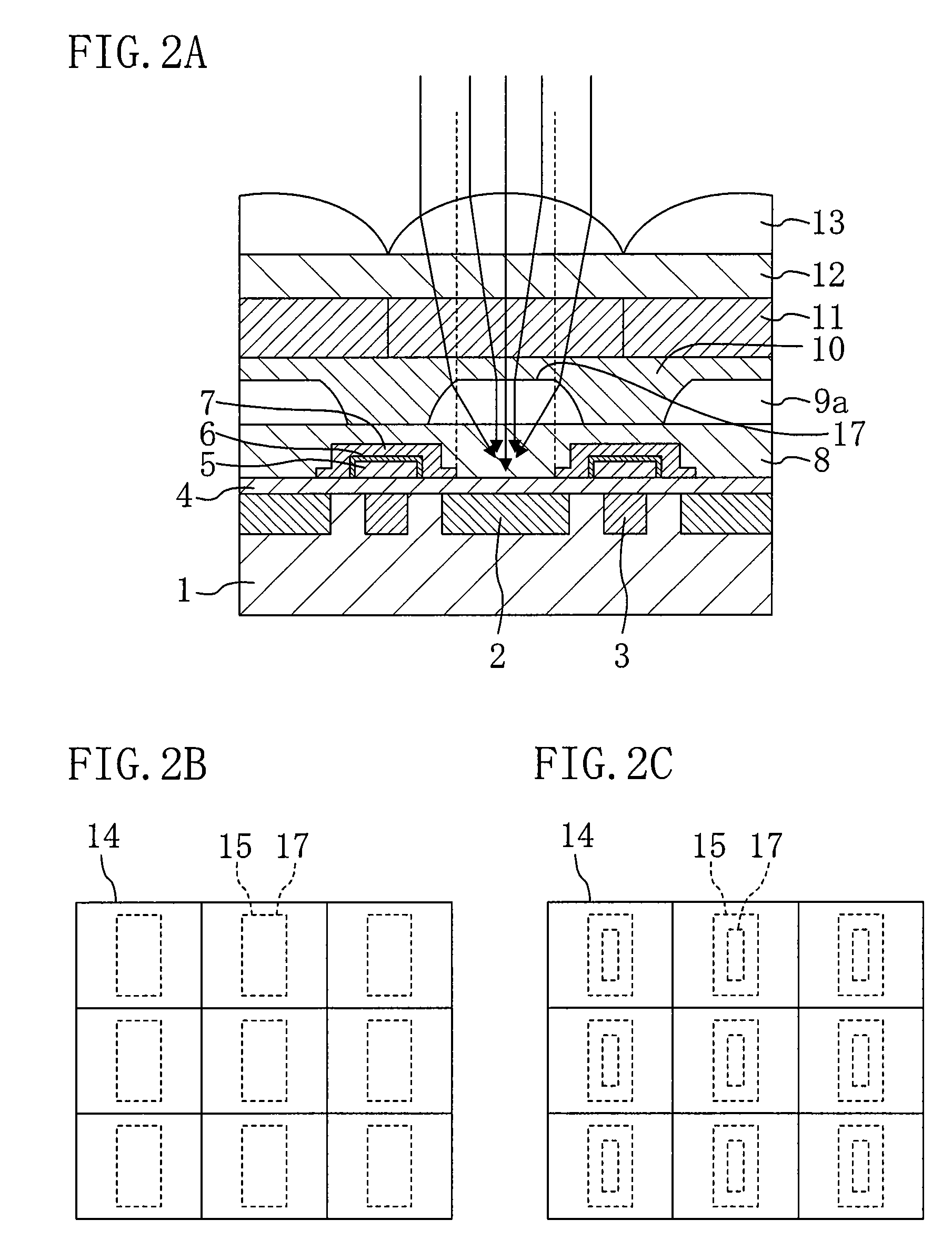
[0057]As shown in FIG. 2A, in the solid-state imaging device of this embodiment, a first microlens 9a and a second microlens 13 each have an upward-convex upper surface. The first microlens 9a has, at a top portion thereof, a flat surface 17 positioned directly above a photoelectric conversion region 2. The flat surface 17 is formed in parallel with a surface of a semiconductor substrate 1. The flat surface 17 will be described in greater detail with reference to FIG. 2B. Note that the solid-state imaging device of this embodiment has a configuration similar t...

third embodiment

[0062]FIG. 3A is a cross-sectional view showing a configuration of a solid-state imaging device according to a third embodiment of the present invention. Note that the solid-state imaging device of this embodiment is different from that of the first embodiment in only a portion of the configuration. Therefore, the same parts as those of the first embodiment are indicated by the same reference symbols and will not be described.

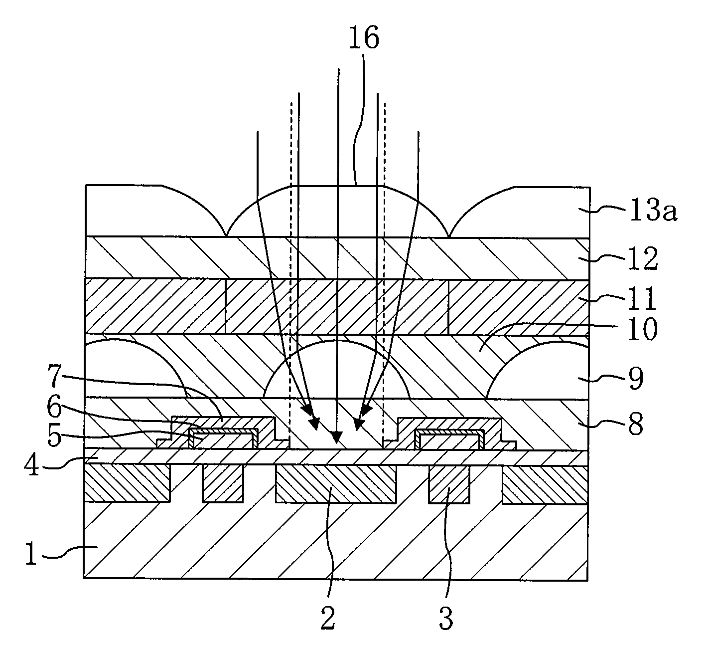
[0063]As shown in FIG. 3A, in the solid-state imaging device of this embodiment, a first microlens 9a and a second microlens 13a each have an upward-convex upper surface. The first and second microlenses 9a and 13a also have, at respective top portions thereof, respective flat surfaces 17 and 16 positioned directly above a photoelectric conversion region 2. The flat surfaces 17 and 16 are formed in parallel with a surface of a semiconductor substrate 1. The flat surfaces 17 and 16 will be described in greater detail with reference to FIG. 3B. Note that the soli...


PUM


Abstract

A solid-state imaging device includes a semiconductor substrate having a photoelectric conversion region, a first microlens provided above the semiconductor substrate, covering the photoelectric conversion region, and having a convex upper surface, for gathering external light into the photoelectric conversion region, and a second microlens provided above the first microlens and having a convex upper surface, for gathering external light into the first microlens. A flat surface is provided at a top portion of one of the first and second microlenses and immediately above the photoelectric conversion region.

Description

CROSS REFERENCE TO RELATED APPLICATION[0001]This application claims priority from Japanese Patent Application JP2008-059434 filed on Mar. 10, 2008, the disclosure of which application is hereby incorporated by reference into this application in its entirety for all purposes.BACKGROUND OF THE INVENTIONDescription of the Related Art[0002]The present disclosure relates to a solid-state imaging device having a microlens and a method for manufacturing the solid-state imaging device.[0003]Solid-state imaging devices for use in digital cameras, camcorders and the like are being modified to achieve a larger number of pixels and further miniaturization so as to increase the resolution of the camera. Since there is a demand for a camera having a still higher resolution, it is expected that the development of a further miniaturized solid-state imaging device having a larger number of pixels will be further accelerated. As the number of pixels of a solid-state imaging device is increased while ...

Claims


Application Information

Patent Timeline
Patent Type & Authority Applications(United States)
IPC IPC(8): H01L31/0232H01L31/18G02B3/00H01L27/14H04N5/335H04N5/359
CPCH01L27/14627
Inventor MATSUSHITA, YOSHIHIRO
Owner PANNOVA SEMIC
Why Eureka
Try Eureka