

Display device
a display device and display technology, applied in the field of display devices, can solve problems such as degrading image quality, and achieve the effect of suppressing flicker and excellent display
- Summary
- Abstract
- Description
- Claims
- Application Information
AI Technical Summary
Benefits of technology
Problems solved by technology
Method used
Image

Examples
first embodiment
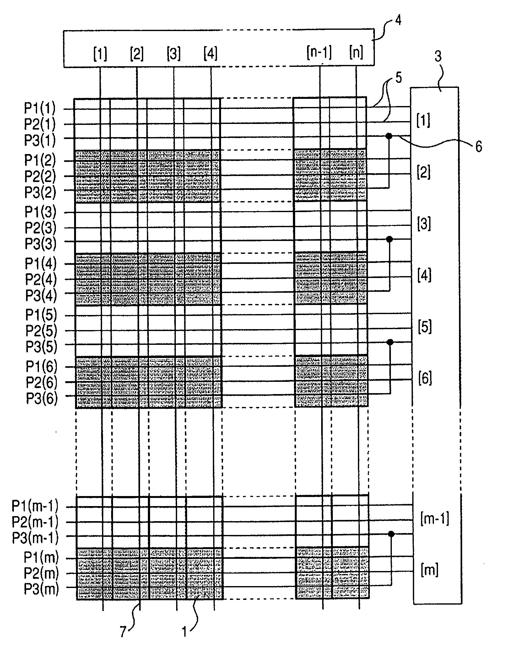
[0049]FIG. 1 illustrates the overall configuration of a display device according to the present embodiment.
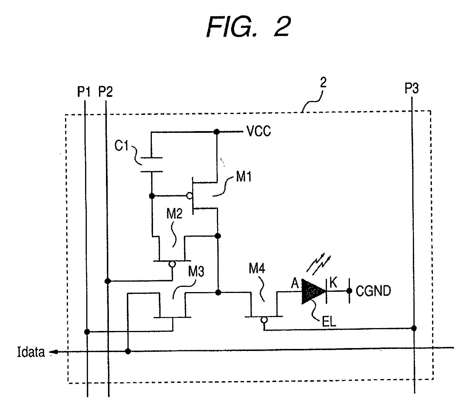
[0050]In FIG. 1, an image display unit includes a pixel 1 formed of an EL element with RGB three primary colors and a pixel circuit composed of TFTs for controlling a current input into the EL element. The pixels are arranged in a matrix of m rows and n columns in the image display unit. A row number “m” is even.
[0051]A row driving circuit 3 and a column driving circuit 4 are arranged at the periphery of a display area.
[0052]The output terminals of the row driving circuit 3 output first scanning signals P1(1) to P1(m) and P2(1) to P2(m) and second scanning signals P3(1) to P3(m). The first scanning signals and the second scanning signals are input into pixel circuits (the circuits 2 in FIG. 2 described later) provided in pixels 1 of each row via first scanning lines 5 and second scanning lines 6 respectively. The second scanning lines 6 of adjacent odd and even rows are commonl...
second embodiment
[0087]The overall configuration of a display device according to the present embodiment is the same as in FIG. 1. The pixel circuit 2 and a method of driving the circuit 2 are the same as those in FIGS. 2 and 3, so that description and figures thereof are omitted.
[0088]FIG. 7 is another timing chart describing another method of driving the display device according to the present invention.
[0089]In FIG. 7, reference characters P1(1) to P1(m) denote the scanning signal P1 corresponding to the first to the m-th row respectively. Reference characters P3(1) to P3(m) signify brightness control signals P3 corresponding to the first to the m-th row respectively. Since the same light emitting period controlling signals are input into the first and the second rows, the third and fourth rows, the fifth and the six rows, and the (m−1)th and the m-th rows, P3(1)=P3(2), P3(3)=P3(4), P3(5)=P3(6), . . . , and P3(m−1)=P3(m). The scanning signals P2 are output in the same timing as described in FIG. ...
third embodiment
[0104]FIG. 11 shows the overall configuration of the display device according to the present invention.
[0105]In FIG. 11, an image display unit includes a pixel 1 formed of an EL element with RGB three primary colors and a pixel circuit 2 composed of TFTs for controlling a current input into the EL element. The pixels are arranged in a matrix of m rows and n columns in the image display unit. Reference characters m and n denote an even number and a natural number respectively. A row driving circuit 3 and a column 4 are provided at the periphery of a display area. The output terminals of the row driving circuit 3C output scanning signals P1(1) to P1(m) and P2(1) to P2(m) and light emitting period controlling signals P3(1) to P3(m). The scanning signals are input into pixel circuits 2 in each row via the first scanning lines 5. The light emitting period controlling signals are input into pixel circuits 2 in each row via the second scanning lines 6. Unlike FIG. 1, the second scanning li...
PUM
 Abstract
Description
Claims
Application Information